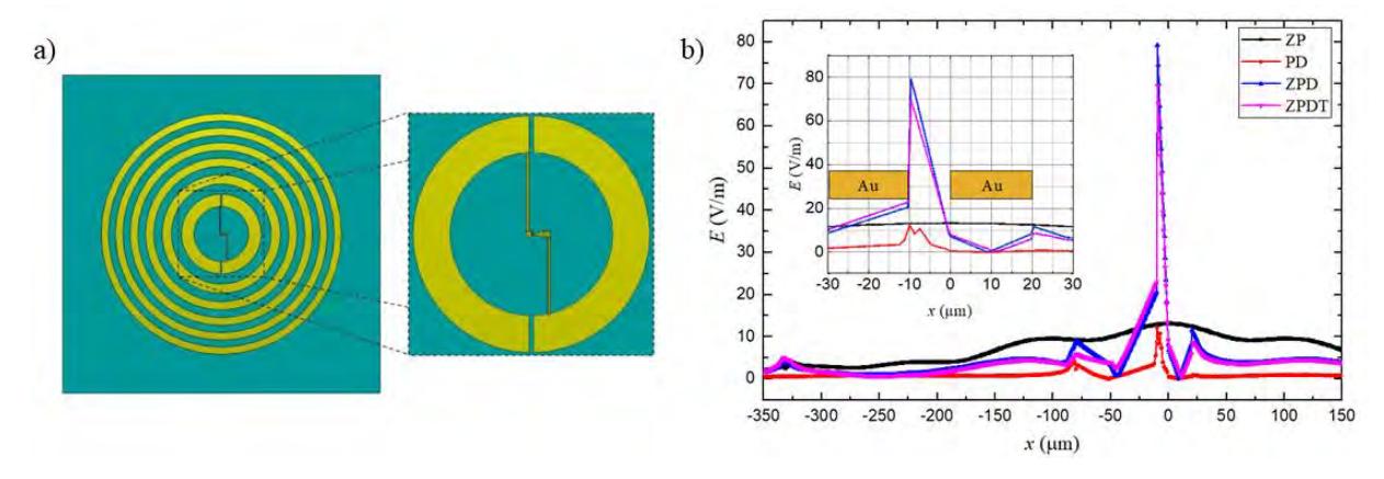
The goal of reducing the dimensions of THz imaging systems is crucial to make them more versatile and practical for various applications such as security or material science [1]. By utilizing wave optics the diffractive optics approach provides a solution to small size, low weight challenge by enabling precise control of phase shifts and constructive interference. The significance of designing diffractive optical elements has grown in recent years as THz beam-forming [2], imaging [3], have become essential in the development of THz technology. By using diffractive optics, it is possible to achieve similar performance to conventional lenses and design elements with a shorter focal length.
The aim of this work is to increase the efficiency of the THz detector by developing design of the radiation coupling optics that maintains the small dimensions of the whole system offering an "on-chip" solution. At the same time, the developed design simplifies the manufacturing technology of the system by bypassing the problem of conform to the planes on both sides of the InP wafer [4].
In this work, models of diffraction optics (zone plates) with InP wafers systems are created using only a computer program CST MW Studio. Various combination of InP wafer thickness and zone plate focal length were virtually created and tested. The best optical part model was integrated with a bowtie THz detector in order to improve the coupling of radiation into the detector. Numerical simulations of terahertz radiation propagation are performed using the same computer program to evaluate the detection system model.
Best performance was demonstrated by 335 µm thickness InP wafer and F = 645 µm zone plate. The obtained results [Fig. 1(b)] shows that bow-tie detector can effectively concentrate electric field by itself. Adding contacts and zone plate around it [Fig. 1(a)] increases electric field 6 times.