Our daily lives are packed with many integrated, functional, and miniaturized devices. The amount of these devices is increasing therefore high demand for fast and cheap manufacturing methods arises. One of the newer methods for molded interconnect devices (MID)[1] production is Selective Surface Activation Induced by Laser (SSAIL)[2], [3]. Technology copes with complex 3D surfaces and allows different materials' metallization by electroless metal plating. However, several challenges related to the selection of optimal surface modification parameters for different surfaces and copper adhesion strength are yet to overcome.
The work is focused on the SSAIL process application on high-performance polytetrafluoroethylene (PTFE) polymer as well as dimensional and electrical properties evaluation of produced electrically conductive copper micro tracks. In this work, two different laser setups with Gaussian and Bessel beams were employed to form conductive microstructures on the Teflon surface. To clarify the best laser modification parameters with a Gaussian beam and the best chemical process steps surface roughness properties including root mean square height (Sq) and core void volume (Vvc) parameters were researched before and after the chemical etching step. After additional sheet resistance measurements, a clear successful metallization window was observed between two threshold values of the irradiation dose (13 and 24 J/cm2) and the highest conductivity was demonstrated for the chemically unetched sample. After the formation of micro tracks with the Bessel beam, it was noticed that metallized micro track's width, formed on the PTFE surface, increases as the scanning speed decreases. Finally, the minimal achievable width of copper-plated conductive micro tracks was evaluated.
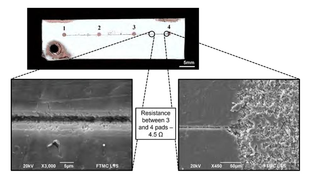
The SSAIL method is successfully applied on the PTFE surface and selective metallized microstructures are formed (Fig. 1). Laser surface modification parameters such as pulse repetition rate and pulse pitch have a huge impact on process selectivity and final conductive track width. Although working sample electrical circuits and conductive micro tracks were experimentally demonstrated, further research on their successful application for conventional electronics is needed.