Several last decades scientists are focused into the miniaturization of the active media of devices thus proceeding to quantum structures like quantum dots, quantum wells, quantum wires and others. These kind of quantum structures tend to be more stable and intensive compared to bulk structures. Moreover, new technique performances allow to manipulate by characteristic parameters of devices applying various technological protocols – different designs of quantum well geometry, interruptions in processes for atom diffusion, ex-situ or in-situ annealing by applying segregation effect, smoothing boundaries of the layers and enhancement of fundamental properties.
AIII-BV-Bi compounds, namely bismides, are relatively new and not fully explored yet. Bismides are one of the most perspective compounds because of their unique properties: fast reduction of energy band gap replacing As by Bi atoms, and low energy band gap dependance on temperature [1]. Although theoretically bismides is looking like very attractive material for NIR applications it has some technological holdbacks. Low epitaxy temperature and close to 1 arsenic and gallium ratio effect leads to poor crystalline quality and weak luminescent properties. Also, bismuth due to large radius tends to segregate to surface even at low growth temperatures.
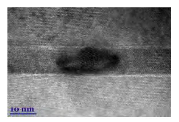
Our microscopical studies of post-annealing treatment demonstrated the formation of Bi nanoparticles emitting in the range of 1000 nm – 1300 nm [2]. The main goal of this work was to study the difference between ex-situ and in-situ annealing for samples grown in Molecular Beam Epitaxy (MBE) reactor. To explore surface and inner layers boundaries differences using atomic force microscopy (AFM) and transmission electron microscopy (TEM) images. Two types of structures with GaAs and AlGaAs barriers were grown. TEM investigation of first type heterostructures showed Bi atoms segregation straight to the surface. To overcome this problem additional ultrathin AlAs barriers were inserted, as Bi atoms blocking layer (see Fig. 1.) It worth noting, that thicker than 1 nm AlAs barriers diminished photoluminescence (PL) intensity. Since these structures will be used for laser source applications, the minimal possible AlAs thickness must be found.