
Si sensors are widely used in CERN experiments for particle tracking [1-4]. However, high energy radiation creates defects that determine the formation of energy levels within the band gap and affect the sensors' operational characteristics [1, 5]. Therefore, new radiation tolerant sensor structures for future experiments are highly desirable. Currently, sensors of pin structure and different types (trip, pixel) are widely employed. However, sensors of pin structure suffer from a decrease in charge collection efficiency. Sensors with internal gain layer (Low Gain Avalanche Detectors - LGADs) [3, 6] appeared to be a promising alternative over sensors of pin structure due to carrier multiplication governed by impact ionization [7] which can compensate the signal drop determined by radiation defects [3]. LGADs are currently being studied within the CERN RD50 program in order to evaluate the changes in sensor parameters after irradiations with high fluences.
This study aimed to examine the recombination and electrostatic characteristics of silicon wafers and junction structures both non-irradiated and irradiated with reactor neutrons and protons of different energies. Microwave probed photoconductivity (MW-PC) transient technique, current-voltage (I-V), and capacitance-voltage (C-V) methods were employed to thoroughly carry out the research.
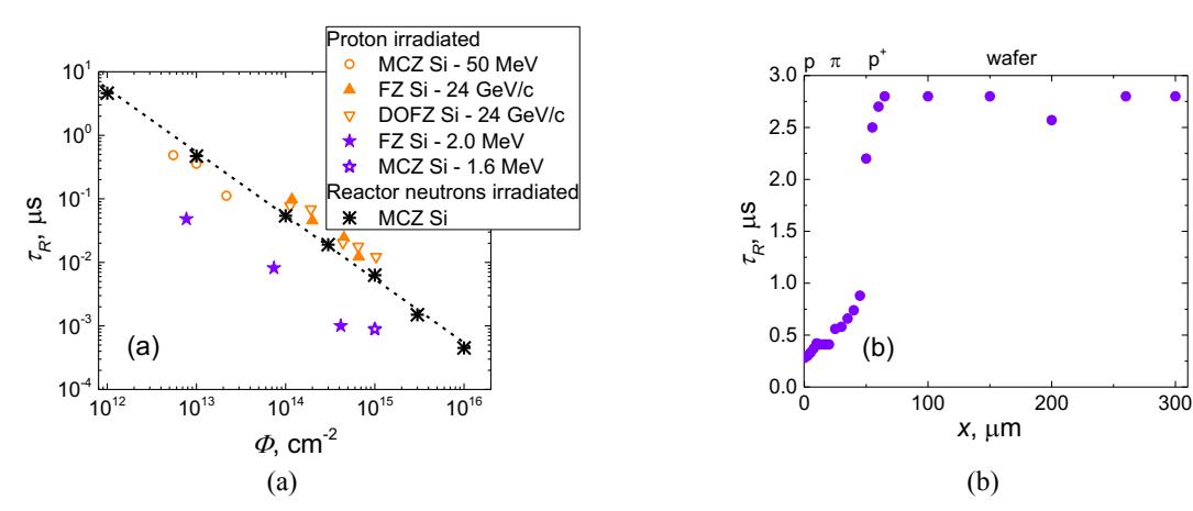
It was determined that carrier lifetime is inversely proportional to fluence due to the increased density of radiation defects in all the investigated samples (Fig. 1(a)). However, carrier lifetime is about an order of magnitude shorter in Si irradiated by stopped protons due to more efficient production of radiation defects at particle penetration depth. The carrier lifetime profiling by edge scanning of microwave-probed photoconductivity transients allowed us to determine the penetration depth of low energy particles. The measurements and analysis of C-V characteristics were used to evaluate the change in the effective density of dopants caused by radiation defects and to determine the penetration depth of the particles stopped within junction structures. Finally, it was shown, that edge scanning of the LGAD sensor structures using a needle-tip microwave antenna and measuring MW-PC transients allows for estimating the charge carrier lifetime tR within individual layers of the structure (Fig. 1(b)).