Only a few percent of bismuth incorporated in GaAs lattice significantly reduces the band gap of the material. Due to attractive properties like large bowing and energy band gap, less sensitive to temperature, bismides are potential material for the applications of optoelectronic devices operating in infrared range such as light-emitting diodes [1], photodetectors [2], solar cells [3] etc. Nevertheless, it is crucial to continue study of GaAsBi and investigate the influence of different designs of quantum structures on the optical properties so that the optimization of future optoelectronic devices could be achieved.
Recently our group [4] developed quantum structure design consisting of GaAsBi quantum wells (QWs) with parabolically graded barriers (PGBs) and a boost in photoluminescence (PL) at room temperature was observed for these structures with 50 times higher PL intensity when compared to conventional rectangular quantum wells. This consequence could be explained by more efficient carrier trapping into the GaAsBi quantum wells and stronger effect of carrier localization. It is important to mention, that enhanced PL intensity is reproducible over the growth conditions in parabolic quantum wells (PQWs).
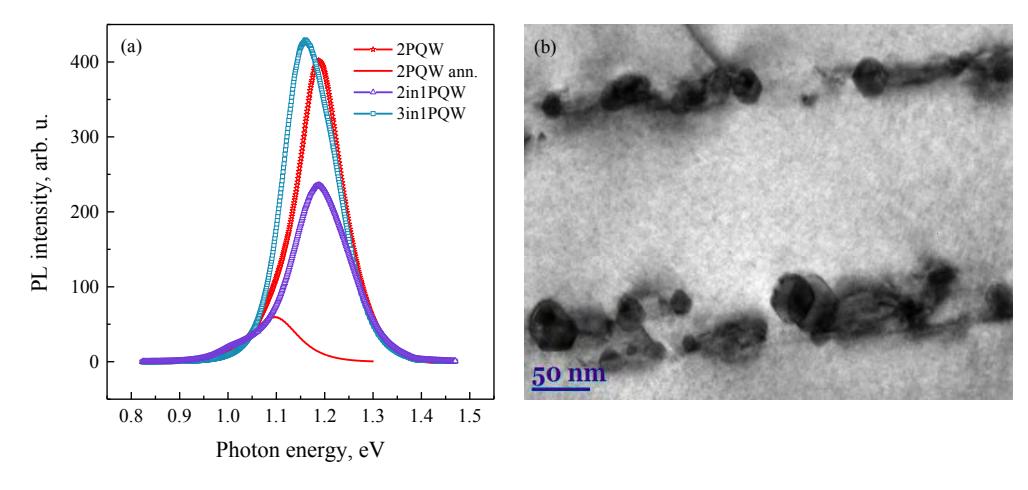
To find a relation between a design of quantum structure and optical properties that they exhibit more comprehensive study of GaAsBi PQWs grown by molecular beam epitaxy (MBE) was conducted. Different designs of two separate parabolic quantum wells (2PQW), two quantum wells embedded together in parabolic barriers (2in1PQW) and three quantum wells embedded together in parabolic barriers (3in1PQW) were investigated and the latest results will be presented in this work. To explore optical properties a widely used technique of photoluminescence was used. The room temperature PL results are presented in Fig. 1 (a). Also, it was shown that thermal annealing could contribute to structural change of a sample. PL spectra of in situ annealed 2PQW structure is redshifted (Fig. 1 (a) red line) at room temperature. In addition, the cross-section transmission electron microscopy (STEM) images (Fig. 1 (b) revealed the formation of Bi nanocrystals during annealing, and increased distortion of the GaAsBi QW layer. Consequently, the PL band of annealed 2PQW structure was assigned to emission from Bi nanocrystals rather than to GaAsBi QW.