
Gallium nitride (GaN) is a binary wide-gap (3.4 eV) and direct-gap semiconductor prospective for formation of modern optoelectronic devices, such as light-emitting diodes, lasers as well as radiation detectors [1,2]. Metalorganic Chemical Vapor Deposition (MOCVD) is commonly used method for growing of crystalline layers of GaN, where the density of dislocations in such layers can reach 1010 cm-2 [3]. These dislocations, being charged and surrounded by space charge region, act as non-radiative recombination centers and also affect the mobility of carriers [4]. The luminescence signals are ascribed to electronic transitions within point defect complexes and depend on the quality of the crystals [5]. The mentioned luminescence bands, ascribed to the point defects, are strongly dependent on temperature, when intensity of scintillation usually increases with cooling of the sample. Manifestation of the luminescence ascribed to electronic transitions within point defect level structure is strongly influenced by dislocations, those density is rather high in MOCVD GaN materials. The wet chemical etching procedures significantly modify the structure of dislocations and their occupied areas and might be the reason of the increase of intensity of scintillation signals in MOCVD GaN based sensors [6]. This work is addressed to consideration of the mentioned phenomena in order to find means for increasing of the MOCVD GaN scintillation signals after modification of dislocations by wet chemical etching.
In this work, the time-integrated (TI) and time-resolved (TR) photoluminescence (PL) characteristics were measured in the 20-300 K temperature range in MOCVD GaN samples chemically etched in orthophosphoric acid (85% H3PO4) with exposure duration of 200 s for each step. Microwave probed photoconductivity (MW-PC) transients were measured for examination of non-radiative recombination characteristics after each etching step.
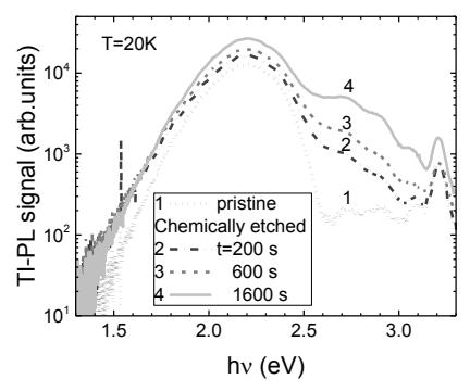
An increase of intensity of the yellow luminescence band (Fig. 1) by a factor of two was observed after modification of MOCVD Ga sample surface by etching with orthophosphoric acid. Additionally, the blue luminescence band appeared within the PL spectra measured at temperatures $T$<200 K in etched GaN samples. The variations of intensity of PL bands might be related to modification of space charge region, surrounding the dislocation cores and acting as non-radiative recombination centers. The variations of PL and MW-PC characteristics in chemically etched MOCVD GaN will be presented and discussed.