Near-infrared is one of the most important spectral regions in current technologies related to compact sensors for consumer electronics, LiDAR, and optical data transfer. GaAsBi is an attractive optoelectronic material for these applications due to its rapid bandgap reduction, ability to suppress Auger recombination, low emission wavelength sensitivity to temperature [1-3]. Even though some GaAsBi-based lasers and LEDs have been realised, the wider application of this alloy is limited by the challenging growth at reduced temperature and low group-V flux resulting in poor crystalline quality. It was noticed that when growing thicker layers (> 30 nm), the GaAsBi growth mode changes and the effective growth rate decreases, thickness deviates from the nominal value. Moreover, a large metallic droplet surface coverage is observed [4-7]. In this work we investigate the peculiarities of growing thick GaAsBi layers focusing on finding the optimal growth condition window for low roughness, high emission intensity at \(\approx\) 1 eV and predictable layer thickness.
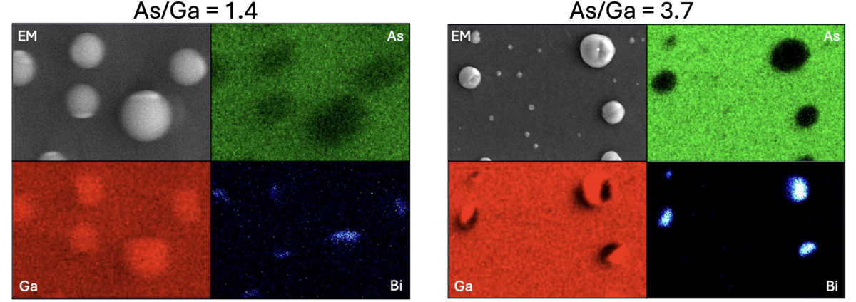
A series of GaAsBi samples were grown using a Veeco GENxplor R&D MBE system while varying the As, Ga and Bi fluxes at \(\approx\) 350 °C substrate temperature. The structural properties were assessed by Nomarski and scanning electron microscopies, energy-dispersive X-ray (EDX) spectroscopy, X-ray diffraction, optical properties were investigated by photoluminescence (PL) spectroscopy. For samples grown in the As to Ga beam equivalent pressure ratio (BEPR) window from 1 to 8 several changes in the growth regime were noticed. In the As/Ga window of 1 to 2, a large metallic Ga droplet surface coverage is observed, pointing to an As deficiency and causing the reduced growth rate. At As/Ga > 3.5 a significant change of surface morphology is observed, with the droplet covered area decreasing by a factor of 8, while the composition of the droplets changes from mostly Ga to biphasic Ga-Bi, signalling the transition away from group-V limited growth. Further increasing the As pressure to As/Ga = 5, an improvement in surface roughness is observed, with very few droplets (d < 250 nm) detected. Additionally, at this point, the PL emission related with transitions in GaAsBi is no longer observed. Finally, at As/Ga > 6, the surface is completely free of metallic droplets, signifying that group-III limited growth conditions are achieved.