During the production of various semiconductor structures, it is sometimes necessary to change the properties of certain layers. This can be achieved by introducing additional defects, thereby changing the chemical or electrical properties of such structures. One of the effective methods for doping and modifying materials is ion implantation. This method of modifying semiconductor materials is one of the essential steps in the manufacturing process of integrated circuits, which form the basis of global communication and advanced computing capabilities [1]. Since the depth of the particles penetrated into the material depends on their energy, it is possible to selectively and locally modify the parameters of the structure only in a certain layer, therefore it is desirable to have the ability to implant various ions in a wide range of ion energies from few keV to several MeV. Therefore, it is essential to determine the elements and molecules sputtered from experimentally measured mass spectra of negative ion beams for different targets in low energy and acceleration branch chambers for further experiments.
In this work, a Tandetron 4100A (General Ionex Corporation, USA) tandem accelerator with a negative ion source Hiconex 834 was used. This technology is based on the use of atoms and molecules knocked out of surfaces, which, when focused into the beam, can be accelerated using high voltage. The particles are knocked out of a conical target of the desired material by a beam of positive cesium ions [2]. To determine the composition of the beam, an analyzing magnet is used, which, by changing the magnetic field strength, can deflect different ions or compounds along different trajectories. By scanning the ion beam at a selected interval, the deflected ions can be selected only by removing all unwanted ions [3]. At the same magnetic field strength, ions with a higher mass/charge ratio deflect less, and ions with a lower ratio deflect more, thus selecting the desired ions by choosing the appropriate magnetic field strength.
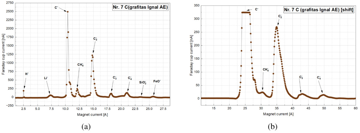
In mass spectrum (Fig. 1) the current value of the analyzing magnet can be used to determine which position the negative ion occupies. This value can be calculated using the formula \(n\sqrt{mE}\), where \(n\) is the coefficient, \(m\) is the atomic mass (a.m.u.), and \(E\) - voltage sum of electronic focusing devices.
The measurements performed in this work can be used to implant negative ions into materials for modification and also to calibrate the parameters of the source equipment.