GaAsBi quantum well (QW) structures are one category of materials currently being studied for active area of light sources operating in the near-infrared (NIR) range [1]. A key advantage of GaAsBi is the strong band-gap redshift with increasing Bi content, together with enhanced spin–orbit splitting that can suppress Auger recombination and inter-valence-band absorption [2]. In addition, GaAsBi shows reduced temperature sensitivity [3], enabling tunable laser operation on the mature GaAs platform without the need for additional cooling. However, complicated growth conditions required for bismides [4] produce a high point-defect density, which degrades crystal quality and luminescence intensity. This has a detrimental effect on emission efficiency and therefore limits the practical implementation of GaAsBi-based optoelectronic devices.
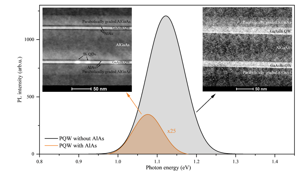
This study investigates how technological modifications, such as, the use of non-conventional graded AlGaAs barriers or thermal treatments affect emission and structural properties of GaAsBi QW structures. We demonstrate that combining QWs with parabolically graded barriers (PQWs) together with optimized in-situ and/or ex-situ annealing can boost emission intensities by 25 times compared to conventional GaAsBi QWs. Annealing, however, promotes Bi redistribution that can distort the quantum structure by degrading the heterointerfaces. To suppress Bi segregation we therefore implemented ultrathin AlAs layers as Bi-blocking barriers. GaAsBi PQWs with these AlAs barriers show improved structural uniformity and even when Bi quantum dots (QDs) form after annealing they do not degrade the heterostructures (see figure 1). Unfortunately, although AlAs layers enhance structural quality, they tend to worsen optical performance of GaAsBi/AlGaAs QWs. The presence of AlAs reduces emission intensity, increases thermal quenching and carrier localization effects. However, this study showed that adverse optical effects introduced by AlAs can be partially mitigated by in-situ annealing and reducing the AlAs barrier thickness. These findings contribute to the optimization of GaAsBi growth processes, paving the way for enhanced optoelectronic device performance in the NIR region.