
Given that today’s dominant solar cells are mostly made from crystalline silicon, the limitations of this technology are becoming increasingly apparent. Also the rigid structure of silicon-based solar cells limits their applications where flexibility or integration into lightweight structures is required. One of the compounds that has received increasing attention in recent years is antimony selenide (Sb₂Se₃). This compound has a suitable energy bandgap ( 1.1–1.2 eV), a high light absorption coefficient, and good electron transport properties. In addition, the composition of Sb₂Se₃ is based on earth-abundant and less toxic elements. However, like many quasi-1D materials, Sb₂Se₃ is an anisotropic compound. To achieve efficient charge transport between the electrodes of a solar cell, it is necessary to form Sb₂Se₃ layers with a predominantly hkl (l≠0) crystallographic orientation. The aim of this work was to control the crystallographic orientation of Sb₂Se₃ thin films to expand the application possibilities of this material in solar cells.
This was achieved by two step synthesis: in the first stage antimony films were deposited using thermal evaporation method, systematically changing process parameters (current, evaporation time and the distance between substrate) to assess their influence on the quality of the layer. The coatings formed on SLG/FTO/TiO₂ substrates were characterized by X-ray diffraction (XRD). In the second stage, the deposited layers were selenized in a rapid thermal treatment (RTA) furnace, and the obtained samples were examined by XRD and scanning electron microscopy (SEM). The analysis allowed us to determine the dependence of the crystal quality, dominant orientation and surface morphology on technological parameters (temperature, time, pressure). 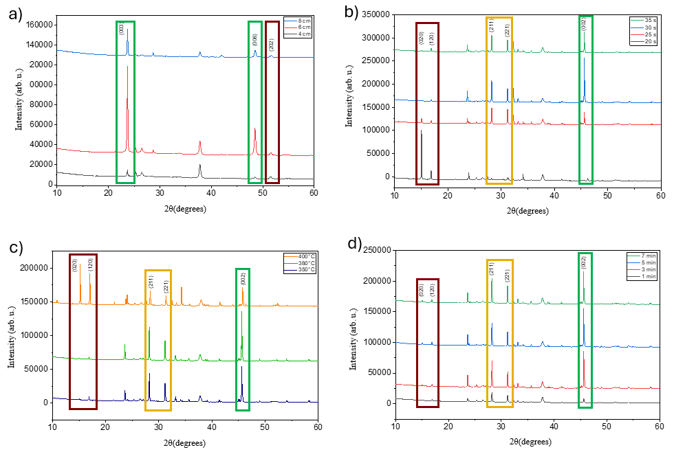
1) The crystallinity of Sb layers directly depends on the distance between the substrate and the precursor material during thermal evaporation.
2) The predominant crystallographic orientation in the Sb₂Se₃ layers directly depends on the crystallinity of the Sb precursor layer.
3) It was not possible to completely avoid hkl (l = 0) oriented Sb₂Se₃ crystal planes, but after conducting a systematic study, we found that samples formed at a distance of 6 cm between the substrate and the precursor material and selenized at 380 ⁰C for 3 minutes are characterized by an extremely low amount of them in the layer.