
Electromagnetic wave-matter interactions are considered fundamental to a wide range of modern photonic and electronic technologies, with particular significance attributed to the terahertz (THz) frequency regime [1] for applications including sensing, imaging, and wireless communication [2]. Within this spectral region, graphene [3] has been identified as a promising plasmonic platform due to its two-dimensional (2D) structure, electrically tunable carrier concentration, and capability to support surface plasmon polaritons (SPPs) exhibiting extreme subwavelength confinement and relatively low damping. A graphene metamaterial absorber (MMA) exhibiting near-unity, electrostatically tunable THz absorption was designed through finite element method (FEM) simulation. Graphene was represented using a surface conductivity formulation derived from the Kubo formalism. For highly doped graphene at THz frequencies, the conductivity is approximated by a Drude-like expression [4]: \[\sigma_g = \frac{e^2 E_F}{\pi \hbar^2} \frac{i}{\omega + i/\tau}\] where, \(\omega\), \(\tau\), \(\hbar\), and \(E_F\) are defined as the angular frequency of the incident radiation, carrier relaxation time, reduced Planck constant, and Fermi energy, respectively. 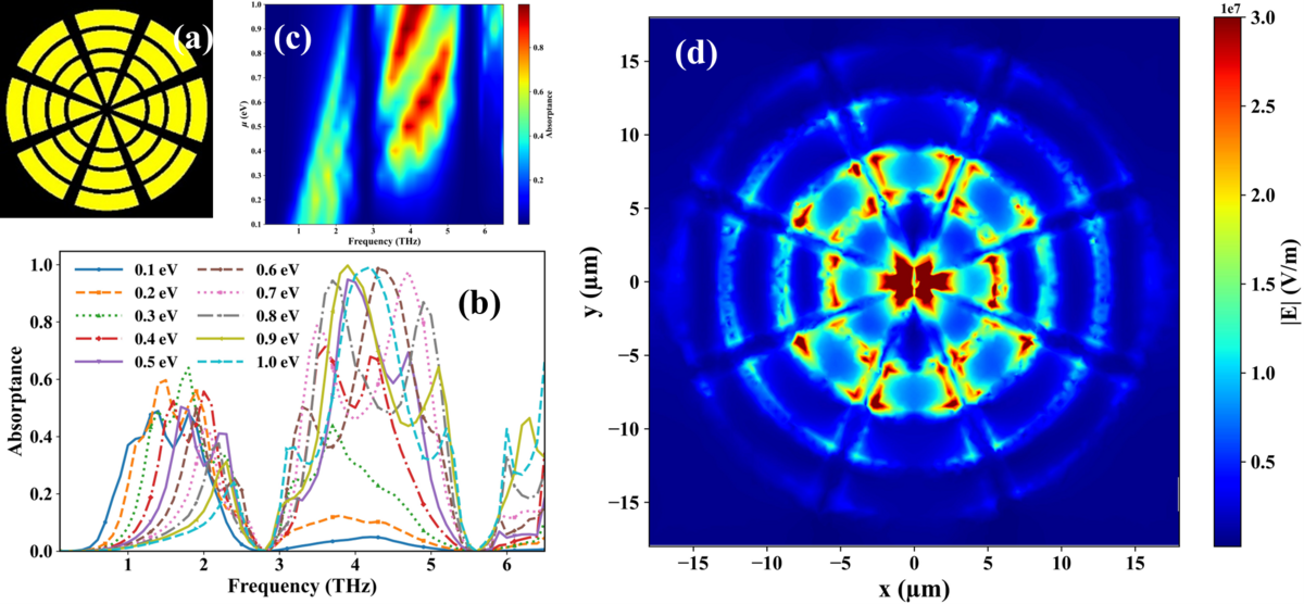
The \(\mu\)–frequency absorption heatmap presented in Fig. 1(c) provides a global representation of this behavior, wherein dispersive absorption bands are observed to shift monotonically toward higher frequencies as \(\mu\) increases. The electric field distribution at resonance (Fig. 1(d)) is characterized by strong confinement within the graphene pattern, through which efficient plasmonic absorption is verified. Collectively, robust electrically tunable near-perfect absorption is demonstrated, and the suitability of the proposed structure for actively reconfigurable THz absorbers is established.