Two-dimensional (2D) materials with atomic-scale thickness exhibit properties arising from quantum confinement and large surface to volume ratios. Thin bismuth (Bi) layers are particularly attractive for topological insulators, sensors, thermoelectric, and ultrafast optical devices. While bulk Bi is a semimetal, films thinner than 30 nm become semiconducting, with bandgaps tunable up to 0.8 eV in the ultrathin limit [1]. Bi growth has previously been demonstrated mainly on InAs, InP, and Si(111), with GaAs(111) also supporting high quality monolayer structures [2–4]. Under femtosecond excitation, Bi films can emit terahertz (THz) radiation through lateral photocurrents and nonlinear effects, while terahertz excitation spectroscopy (TES) enables investigation of band structure and carrier dynamics.
In this work, Bi layers were grown by molecular beam epitaxy on (100) oriented GaAs, a substrate orientation not previously reported. Heterostructures with 9 nm thick Bi layers were fabricated on semi-insulating, n-type, and p-type GaAs substrates. THz emission was studied as a function of excitation photon energy using femtosecond laser pulses in reflection geometry, with p-polarized light incident at 45° and constant average power of 20 mW. The excitation wavelength was tuned using an optical parametric amplifier.
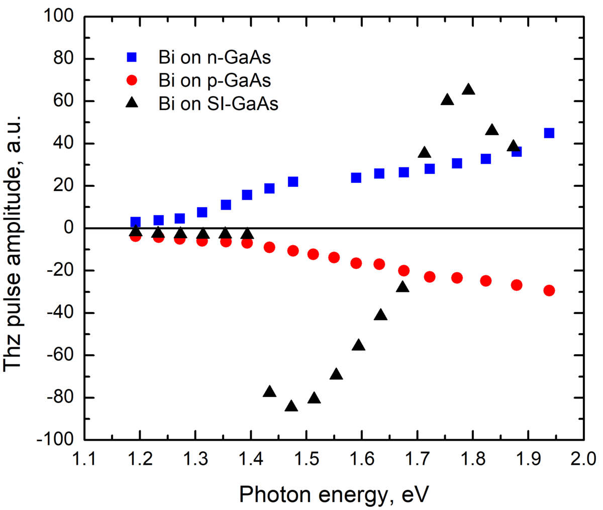
The TES spectra revealed pronounced doping dependent behavior. Strong THz emission appeared only when photon energy exceeded the GaAs bandgap (1.42 eV), indicating that the dominant contribution originates from carrier dynamics within the GaAs substrate. Below this threshold, detectable THz emission was observed only for Bi/n-GaAs heterostructures. Opposite THz pulse polarities from n-type and p-type substrates were attributed to reversed internal electric fields at the Bi/GaAs interface, which drive photocurrent transients in opposite directions. Comparison with bare GaAs substrates estimated of the Bi optical absorption coefficient between 3×10⁵ cm⁻¹ and 4×10⁵ cm⁻¹ in the 1.5–1.7 eV range, which is over an order of magnitude higher than that of GaAs [5]. More pronounced deviations were observed for Bi semi-insulating GaAs, where excitation through the Bi layer reduced THz amplitude and reversed polarity near 1.7 eV, suggesting an additional emission mechanism associated with strong interfacial electric fields. Notably, Bi/p-GaAs heterostructures exhibited enhanced THz emission relative to bare p-GaAs, attributed to hole velocity overshoot in the strong internal electric field. Overall, thin Bi layers substantially modify THz emission through enhanced optical absorption and altered band alignment, highlighting Bi/GaAs heterostructures as promising platforms for efficient surface THz emitters.