
Gallium nitride (GaN) is a wide-bandgap semiconductor studied for radiation detection, optoelectronic, and high-power electronic applications due to its high radiation hardness, thermal stability, and favorable carrier transport properties [1]. In GaN PIN detector structures, precise control of dopant incorporation and free carrier concentration in epitaxial layers is essential for achieving stable and reproducible electrical performance, yet remains technologically challenging, particularly for p-type doping.
In this work, Si-doped n-GaN and Mg-doped p-GaN epitaxial layers were grown by metal–organic chemical vapor deposition (MOCVD) under varied growth temperature, pressure, and dopant precursor flow conditions. Dopant and background impurity concentration profiles were determined by secondary ion mass spectrometry (SIMS), while Hall effect measurements were employed to evaluate free carrier concentration and electron mobility in n-GaN layers. Comparison of n-GaN SIMS and Hall data reveals the influence of background donor impurities and parallel conduction paths, particularly at low intentional doping levels.
The results demonstrate that Si-doped n-GaN exhibits controllable dopant incorporation over a wide concentration range of approximately 10\(^{17}\) – 10\(^{19}\) cm\(^{-3}\), with electron mobility values reaching up to 300 cm\(^{2}\)/V⋅s under optimized conditions. While optimized growth conditions provide the highest electron mobility, growth at elevated temperature and reduced pressure produces more uniform electrical properties across the sample surface (Fig. 1.).
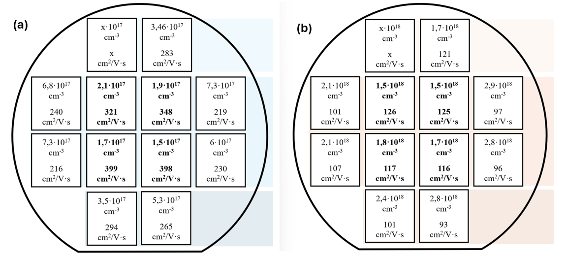
Additionally, Mg-doped p-GaN layers exhibit Mg concentrations sufficiently high for p-type operation (up to 10\(^{20}\) cm\(^{-3}\)). Nevertheless, p-type doping remains challenging due to pronounced Mg memory effects, resulting in significant Mg incorporation even in nominally undoped layers.