Terahertz (often defined as 100 GHz – 10 THz frequency range of the electromagnetic spectrum [1]) has the ability to penetrate non-conductive materials, it is non-ionizing in nature, and it has resonance with the rotational and vibrational modes of complex biomolecules. These properties are of interest for the development of high-power THz sources and high-sensitivity THz detectors. Field-effect transistors (FETs) with integrated antennas are being used in development of such THz radiation detectors [2]. FET technology is compatible with commercial complementary metal–oxide–semiconductor manufacturing processes and can operate efficiently at room temperature.
This work outlines the development of terahertz sensors based on FET technology and studies on their angular characteristics while operating at 2.52 THz.
This study involved several stages of detector development, including the investigation of suitable low‑noise amplifier components, amplifier circuit modeling to validate the expected behavior, component soldering, and the assembly of the complete sensor device. Then, measurements were carried out to determine the angular dependency of detected power and scanning the antenna area using a mirror system that guided the THz wave from a 2.52 THz source.
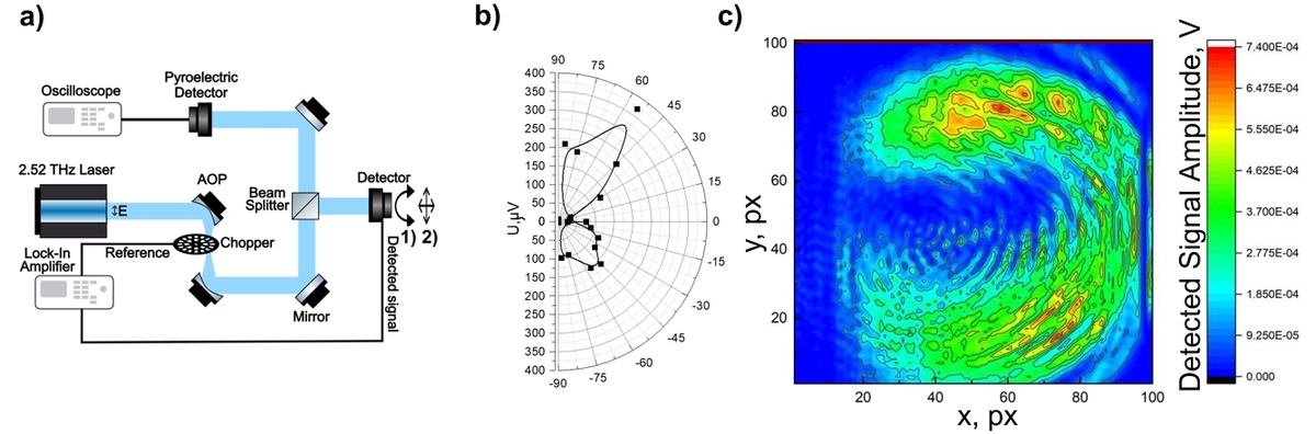
The principle measurement diagram is shown in Fig. 1(a)). It depicts the laser used, the mirror system and the detector, which underwent both angular measurement (1)) and signal intensity mapping (2)). The conducted angular measurements (Fig. 1 b)) revealed an asymmetric, multi-lobed response peaking at 55° (370 μV) and −45° (161 μV). These results prompted a signal mapping (Fig. 1 c)) to determine why they differed from the expected Gaussian result. The spatial mapping revealed a doughnut-shaped terahertz beam with a central minimum, also observed in [3] for the same laser.
The future experiments will aim to involve the pinhole method at the intermediate focus, which will eliminate the modes and reduce their influence on beam profile characterisation.