Antimony selenide (Sb₂Se₃) is a one-dimensional crystalline material comprised of non-toxic and earth abundant elements. The band gap of this semiconductor is approximately 1.2 eV, the electron mobility in single crystals is between 10 and 40 cm²V⁻¹s⁻¹, and absorption coefficient exceeds 10⁴ cm⁻¹ above the band gap. Due to these properties, Sb2Se3 has attracted considerable scientific interest for use in photovoltaic technologies, including thin-film solar cells, photodetectors, and photoelectrochemical systems. [1, 2]
A suitable electron transport layer material for fabricating Sb₂Se₃ solar cells is zinc oxide (ZnO) due to its tunability via magnesium doping, which allows control of optoelectronic parameters, such as the band gap, conduction band offset, carrier concentration and optical transmittance [3]. However, Sb₂Se₃ is rarely synthesized on ZnO layers, particularly using vapor deposition techniques. Despite the suitable properties of ZnO, the detailed physical and interfacial properties of this heterojunction remain underexplored.
In this work, the Sb₂Se₃ absorber was deposited by vapor transport deposition (VTD) in a three-zone tube furnace onto spin-coated ZnO substrates. The growth conditions were systematically varied, including the substrate temperature (400–520 °C), distance of the substrate from the heating zone (−4 to 0 cm), deposition duration, arrangement of evaporation source. The deposited samples were characterized using standard structural characterization techniques, including scanning electron microscopy (SEM), X-ray diffraction (XRD), and complementary optical and electrical measurement methods.
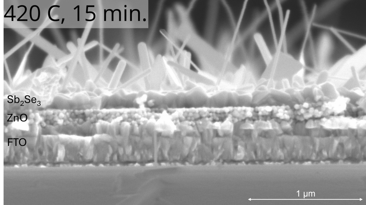
SEM analysis shows distinct variations in the morphology of the Sb₂Se₃ films between samples grown under varying conditions. When the source powder was placed in the middle zone of the furnace, decreasing the temperature from 440 °C to 420 °C resulted in an increase in whisker formation on the Sb₂Se₃ layer. In contrast, when the source powder and the substrate were positioned within the same furnace zone, the lower temperatures produced lower density of whiskers and higher open circuit voltage than samples grown in higher temperatures. Samples grown at 400 °C for 15 minutes exhibited poorer electrical performance compared to those grown for 30 minutes, indicating that the optimal growth conditions are at low temperature with a longer deposition process.