Optical properties of polar nitride quantum well (QW) structures are strongly influenced by the internal electric field arising from both spontaneous and piezoelectric polarizations [1]. In light-emitting diodes (LEDs), the active region QWs are sandwiched between p-type and n-type layers. The net electric field in the wells is therefore a superposition of the intrinsic polarization field and the junction field. This combined field distorts the QW potential, spatially separates electron and hole wavefunctions, and reduces the radiative recombination efficiency. One approach to mitigating these negative effects is the introduction of doped barriers [2,3], which can partially screen the polarization charges. The aim of this work is to investigate photoluminescence (PL) dynamics in InGaN/GaN QWs with varying structural parameters and junction configurations.
Eight InGaN/GaN QW structures grown by metal-organic chemical vapor deposition (MOCVD) on sapphire substrates were studied. The samples were divided into two groups, p-n and n-n, based on the barrier doping configuration. Each group contained four samples with QW widths ranging from 2.0 nm to 7.0 nm. The structures were characterized using PL spectroscopy with a 405 nm CW laser diode as the excitation source. Temperature-dependent PL measurements were performed under low excitation conditions in the range of 8-300 K, while excitation-dependent PL was measured at power densities from 32 mW/cm2 to 20 W/cm2.
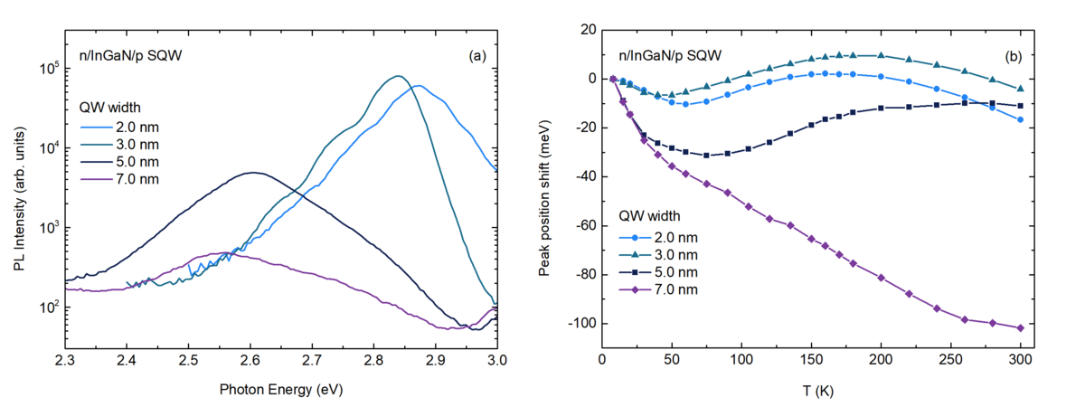
The room-temperature PL spectra of the p-n InGaN/GaN QWs exhibit the redshift of the emission peak and spectral broadening as the QW width is increased (Fig. 1a). While PL intensities remain similar in narrow QWs, they decrease significantly in the wider structures. The characteristic S-shaped temperature dependence of the peak position shift (Fig. 1b) indicates strong carrier localization. Local minimums occur at different temperatures for different QW widths, and the magnitude of the redshift becomes more pronounced in the wider structures. For the widest QW, no local minimum is observed within the measured temperature range, suggesting a very broad distribution of localized states. A comparison of the two studied sample groups reveals similar trends for the n-n structures.
The obtained results indicate that, under low excitation conditions, the PL properties of the studied samples are governed primarily by the physical QW parameters rather than by the junction configuration.