IMPACT OF RAPID THERMAL ANNEALING ON STRUCTURAL AND OPTICAL PROPERTIES OF GaAsBi/(Al,Ga)As QUANTUM WELLS
Patricija Strumilaitė1, Aivaras Špokas1, Justas Žuvelis1, Andrea Zelioli1, Sandra Stanionytė1, Kipras Mažeika2, Augustas Vaitkevičius1, 2, Renata Butkutė1, Evelina Dudutienė1
1 SRI Center for Physical Sciences and Technology, Department of Optoelectronics, Lithuania
2 Vilnius University, Faculty of Physics, Institute of Photonics and Nanotechnology, Lithuania
Replacing a small fraction of As atoms in the GaAs lattice by Bi strongly reduces the band gap energy (E\(_{g}\)) and significantly suppresses its temperature dependence [1,2]. These properties make GaAsBi quantum structures promising for active regions of near-infrared light-emitting devices. However, the very low growth temperatures required (< 440 \(^{o}\)C [3]) increase defect density and reduce photoluminescence (PL) efficiency [4]. Post-growth annealing is commonly used to improve epitaxial layer quality, yet its effects on GaAsBi remain controversial [5,6] and requires further investigation.
In this work, optical properties of GaAsBi/(Al,Ga)As multiple quantum well (MQW) structures grown by molecular beam epitaxy (MBE) were investigated using PL spectroscopy. The Bi concentration ranged from 8 to 11 %. Post-growth annealing was performed in a rapid thermal annealing (RTA) furnace under nitrogen atmosphere at 550, 600, 650, 700, and 750 \(^{o}\)C for 3 minutes. Structural and morphological properties were additionally examined using high-resolution X-ray diffraction (XRD) and atomic force microscopy (AFM).
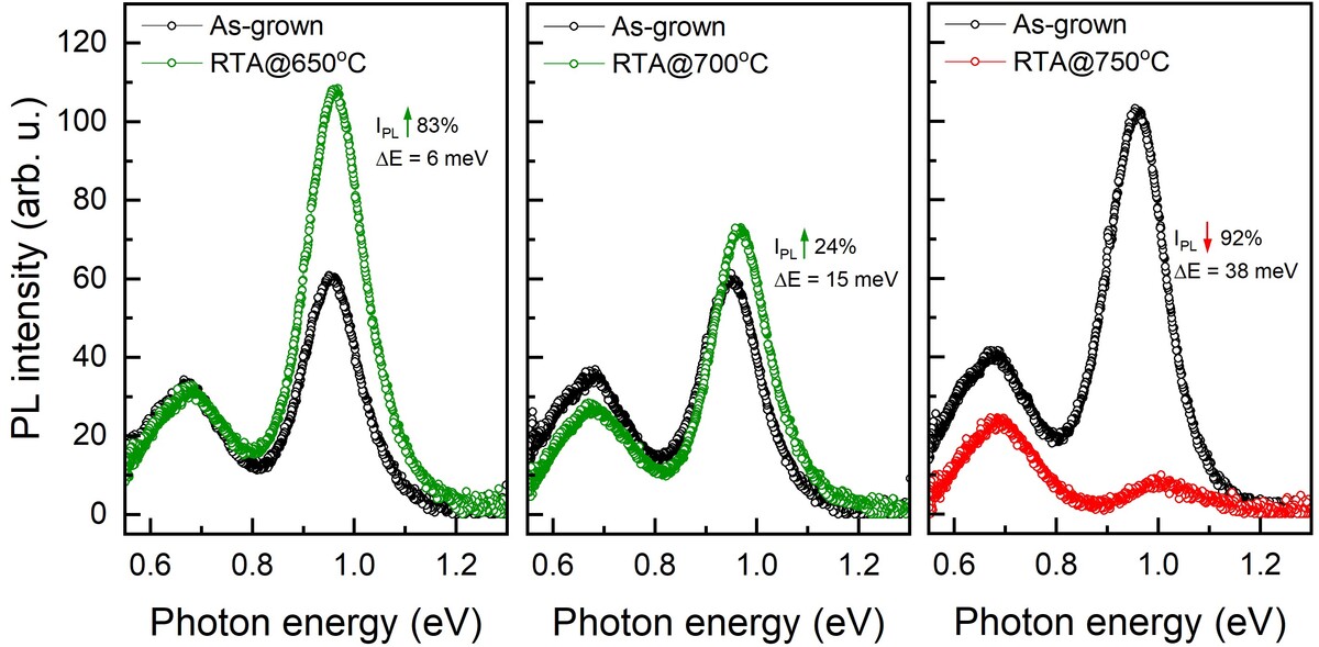
Annealing GaAsBi MQW with GaAs barrier resulted in degradation of crystalline and optical properties at all investigated temperatures. This behavior is attributed to Bi segregation from the GaAsBi to the surface, disrupting the periodic GaAsBi/GaAs structure. In contrast, GaAsBi MQW with AlGaAs barriers exhibited enhanced optical performance upon annealing at 650 \(^{o}\)C and 700 \(^{o}\)C, with PL intensity increases of 83% and 24%, respectively, indicating improved crystalline quality and effective Bi confinement. Annealing above 700 \(^{o}\)C degraded the optical properties of all samples. A blueshift of the PL emission was observed in all structures annealed above 600 \(^{o}\)C, indicating a reduction of Bi content in the GaAsBi lattice. Although literature reports suggest Bi quantum dot (QD) formation during annealing [7], no QD-relate emission was detected from 4 K to 300 K, implying an insufficient concentration of optically active Bi nanocrystallites.
Fig. 1. Room-temperature PL spectra of GaAsBi/AlGaAs MQW before and after RTA at different temperatures.
Acknowledgments: This research has received funding from the Research Council of Lithuania (LMTLT), agreements No. S-SV-25-203 and No. S-MIP-24-99.
[1] S. Francoeur et al., “Band gap of GaAs1−xBix, 0<x<3.6%,” Applied Physics Letters, vol. 82, no. 22, pp. 3874–3876, May 2003, doi: 10.1063/1.1581983.
[2] K. Alberi et al., “Valence band anticrossing in GaBixAs1−x,” Applied Physics Letters, vol. 91, no. 5, Jul. 2007, doi: 10.1063/1.2768312.
[3] R. D. Richards et al., “Molecular beam epitaxy growth of GaAsBi using As2 and As4,” Journal of Crystal Growth, vol. 390, pp. 120–124, Dec. 2013, doi: 10.1016/j.jcrysgro.2013.12.008.
[4] A. Štaupienė et al., “Internal quantum efficiency of GaAsBi MQW structure for the active region of VECSELs,” Applied Physics Letters, vol. 125, no. 22, Nov. 2024, doi: 10.1063/5.0234853.
[5] P. C. Grant et al., “Rapid thermal annealing effect on GaAsBi/GaAs single quantum wells grown by molecular beam epitaxy,” Journal of Vacuum Science & Technology B Nanotechnology and Microelectronics Materials Processing Measurement and Phenomena, vol. 32, no. 2, Mar. 2014, doi: 10.1116/1.4868110.
[6] B. Čechavičius et al., “Thermal annealing effect on photoexcited carrier dynamics in GaBixAs1−x,” Semiconductor Science and Technology, vol. 26, no. 8, p. 085033, Jun. 2011, doi: 10.1088/0268-1242/26/8/085033.
[7] R. Butkutė et al., “Bismuth Quantum Dots in annealed GaAsBi/AlAs Quantum Wells,” Nanoscale Research Letters, vol. 12, no. 1, p. 436, Jun. 2017, doi: 10.1186/s11671-017-2205-7.