
Glass micropatterning is important in many novel technologies, such as microfluidics or fabrication of metasurfaces [1, 2]. This work investigated the possibility of fabricating microstructures in glass using direct laser interference ablation and wet chemical etching through a thin chromium mask. The fabrication process consists of three steps: selective removal of chromium film, using laser, etching through glass surface, removal of chromium film (Figure 1a). Using laser, holes were ablated in thin chromium film. Then the samples were etched in KOH solution for different time intervals. Lastly, chromium layer was dissolved in chromium etchant. After the experiment, the samples were investigated using Sensofar optical profiler, where the channel depth and its entrance width data were obtained. Dependence of dimple depth on number of pulses per spot (Figure 1b) and irradiation fluence was found. 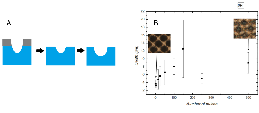
FORMATION OF MICROSTRUCTURES IN GLASS USING LASER INTERFERENCE ABLATION AND CHEMICAL ETCHING
Daumantas Sriubas1, Simonas Indrišiūnas2
1 Vilnius University, Faculty of Physics, Center for Physical Sciences and Technology, Department of Laser research, Vilnius, Lithuania
Fig. 1. a – fabrication of microstructures in glass using direct laser interference ablation and wet chemical etching after removing a thin chromium mask; b – dependence of microstructures depth on number of laser pulses per spot.
[1] 1. Patrice Genevet, Federico Capasso, Francesco Aieta, Mohammadreza Khorasaninejad, and Robert Devlin Recent advances in planar optics: from plasmonic to dielectric metasurfaces, Optica, 4(1), pp. 139-152 (2017).
[2] 2. Felix Sima and Koji Sugioka. "Ultrafast laser manufacturing of nanofluidic systems" Nanophotonics, (9), pp. 2389-2406, (2021).