Emitters designed for the near-infrared (NIR) are essential for a wide variety of applications, spanning optical communications, medical imaging, and remote sensing. However, achieving efficient NIR emission, especially beyond 1 µm, on the GaAs platform remains challenging. The most widely used material system in this spectral region is InGaAs/GaAs quantum wells (QWs). However, device performance is limited by Auger recombination and the necessity for high indium content, resulting in degraded optical efficiency due to misfit dislocations [1]. An attractive alternative for NIR emission is GaAsBi. By substituting arsenic atoms with bismuth (Bi), the bandgap shrinks by 60-90 meV per % Bi, and above 10.5 % Bi the spin–orbit splitting energy exceeds the bandgap, suppressing a prominent Auger recombination channel [2]. Although achieving high crystalline quality remains challenging, growth optimization and rigorous studies over the past decades have enabled the fabrication of light-emitting devices (LEDs) and laser diodes [3]. Therefore, it is increasingly important to evaluate GaAsBi-based emitter performance under electrical injection.
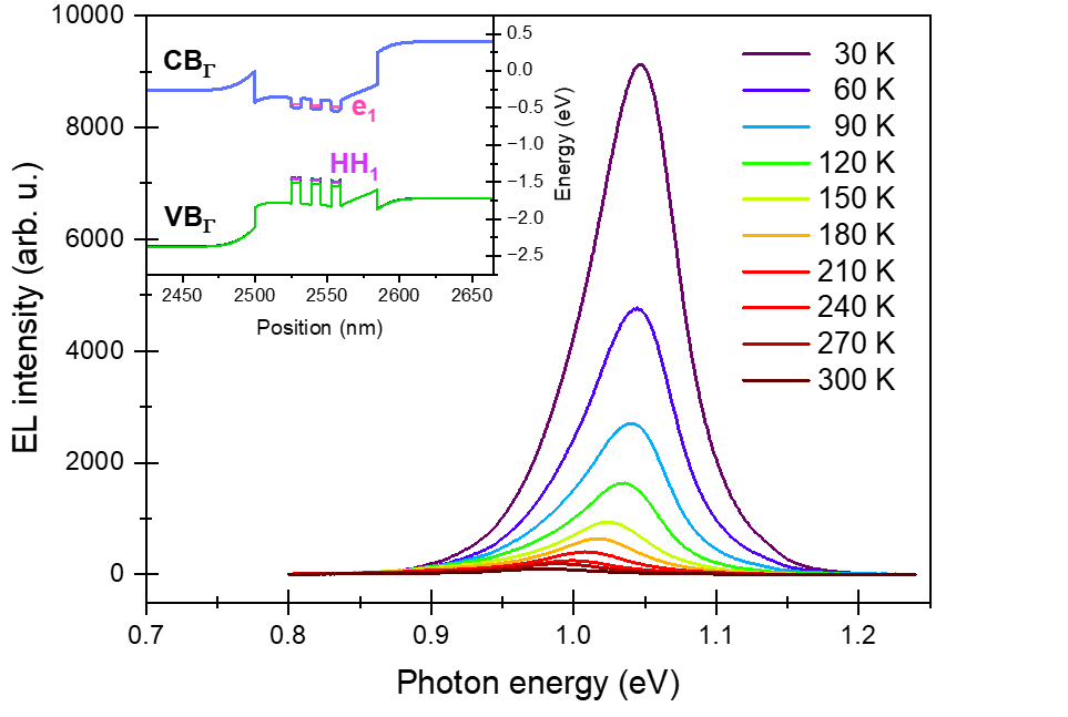
In this work, temperature-dependent electroluminescence (EL) spectroscopy is used to characterize several molecular-beam-epitaxy grown LED and laser-diode structures with different GaAsBi active-region designs (see Fig. 1). The study focuses on quantifying how the emission wavelength and intensity depend on operating temperature and drive current, and on evaluating the internal quantum efficiency [4]. In addition, photoluminescence measurements are done to assess how the dominant recombination channels change under electrical injection. The optical investigation is further supported by electronic-structure modeling using the nextnano software, shown in the inset of Fig. 1, which enables estimation of the Bi content and provides insight into carrier confinement within the device structures.