Silver bismuth sulfide (AgBiS\(_{2}\)) has recently emerged as a promising, non-toxic light absorber material for thin-film photovoltaic applications due to its suitable optoelectronic properties and earth-abundant elemental composition [1]. AgBiS\(_{2}\) has demonstrated exciting potential to be used in photovoltaics, as solar cells employing silver bismuth sulfide have achieved power conversion efficiencies exceeding 9% [2]. Many current methods of AgBiS\(_{2}\) deposition rely on advanced and complex technology, such as atomic layer deposition (ALD), while physical vapor deposition routes offer reproducibility, low manufacturing costs, and an industrially applicable procedure. This opens the door to further optimize this technology through a larger and scalable process.
In this research, we investigate the growth of AgBiS\(_{2}\) by employing physical vapour deposition routes. Glass substrates were first coated with molybdenum (Mo) by thermal evaporation, which acts as a back contact, onto which all films were subsequently deposited. Additionally, the formation of a MoS\(_{2}\) layer beneath the absorber film during sulfurization can be beneficial by serving as a hole transport layer if properly optimized. Layers of silver (Ag) and bismuth (Bi) were deposited by e-beam evaporation and thermal evaporation, respectively. The Ag/Bi stack sequence, ratio, and total thickness were varied. The silver layer thicknesses of 6.5, 9.5, and 19 nm and the bismuth layer thicknesses of 13.7, 20, and 40 nm were employed, corresponding to the total stack thicknesses in the range of 20.2–69 nm, while expecting the AgBiS\(_{2}\) thickness in the range of 35-100 nm. All layers were obtained on 1.5 x 2 cm\(^{2}\) substrates. Furthermore, large area 5 x 10 cm\(^{2}\) samples were fabricated by fixing the thickness of one metal layer while depositing a thickness gradient of the other (Ag or Bi). Large-area samples were employed to investigate the effect of the Ag/Bi stack ratio. Sulfurization of the deposited stacks was subsequently carried out as a reactive annealing in a tubular furnace over a temperature range of 300–500 °C for 30 min.
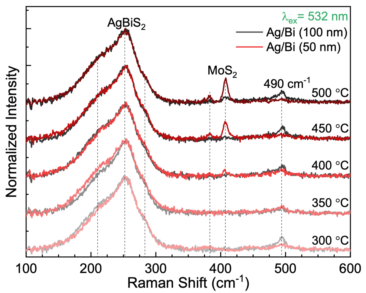
All samples were characterized by X-ray diffraction (XRD) analysis, Raman spectroscopy, and Scanning Electron Microscopy (SEM). XRD analysis reveals crystalline and preferred phases of AgBiS\(_{2}\) with no significant influence in the Ag/Bi versus Bi/Ag sequence, Raman spectroscopy suggests the formation of MoS\(_{2}\) at temperatures of 450 and 500 °C, and SEM analysis indicates homogenous film morphology in thicker stacks.