
Several types of lasers, such as, solid-state, semiconductor, gas, excimer, and dye lasers, have been developed. Today lasers are used in many fields, particularly in optical fiber communication, optical digital recording, material processing, biology and medicine, spectroscopy, imaging, entertainment, and many others. Due to exceptional material properties and/or investigation conditions various application require unique set of laser parameters - emission wavelength, its tunability, beam quality, operation temperature, optical output power, as well as convenient method of laser excitation, power consumption, high-speed modulation and device size is very important.
Vertical-external-cavity surface-emitting lasers (VECSEL) also called optically pumped semiconductor lasers (OPSL) or semiconductor disk laser (SDL) belong to relatively new laser family that combines many of the desirable properties. VECSELs were developed to overcome key problems typical to conventional semiconductor lasers. In comparison to both types of electrically pumped Vertical-cavity surface-emitting lasers (VCSELs), which emit circular fundamental transverse mode beam but exhibit low power and edge emitting lasers (Fabry-Perot and DFB) that can reach high output power but an asymmetric beam with strong angular divergence, VECSELS are capable to generate high optical power with circular beam quality.
In this work the main activity was focused to investigation of the technological parameters required to grow high quality GaAsBi quantum structures, balance the strain during the growth procedure, obtain sharp interfaces and investigate photoluminescence properties. The multiple quantum well structures were grown using solid-source MBE system (Veeco GENxplor R&D) equipped with standard cells for metallic Al, Ga, Bi and unique As design source generating arsenic dimers flux. The semi-insulating GaAs substrate oriented in (001) crystalline plane was selected for the growth of the structures. During this work the thickness of the quantum wells has been kept constant at 10nm. Fig. 1 demonstrates two different geometries of quantum wells investigated in this work. The design of sample shown in Fig. 1a consists of two separated quantum wells with parabolic barriers of AlGaAs. While sample b contains three quantum wells separated by usual shape GaAs barriers enclosed by AlGaAs parabolic barriers.
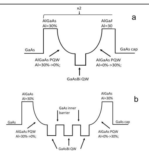
To obtain high crystalline quality and enhanced optical properties of MQW structures the temperature of the substrate was varied from 420 °C to 425 °C, and the beam equivalent pressure ratios of Bi/Ga as well As/Ga were changed in the ranges of 1.05-1.10 and 0.4-3.0, respectively.
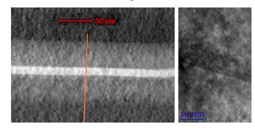
The HR-TEM and STEM investigation evidenced that GaAsBi QWs with AlGaAs PQBs were formed successfully (see Fig. 2). The profiling of atomic composition measured along growth direction (orange line) confirmed the parabolic Al increase and decrease in barriers and step-like Bi profile in QW. The microscopy pictures presented in Figure 2 shows typical cross-sections of GaAsBi QW surrounded by parabolic AlGaAs barriers and zoomed TEM picture of GaAsBi QW. Visible atomic columns in fig. 2 left picture illustrates the highest crystalline quality of grown samples with no defects and dislocations.
The photoluminescence measurements determined the relationship between the growth conditions and emission energy and intensity and highlighted the crucial growth parameters - As/Ga beam equivalent pressure ratio, Bi flux, growth rate and substrate temperature.