The engineering of new materials exhibiting synergy of electro-optical properties in the near infrared (NIR) spectrum region has attracted a lot of attention of scientific community in the last decade. On the other hand, the scientists are focused into the reduction of the active media dimensions by proceeding to quantum nanostructures like quantum dots, quantum wells, quantum wires etc. Minimization of dimensions (optimization of the quantum well geometry) induces quantum effects, which opens the opportunity to technologically manipulate characteristic parameters of the device, while applying various technological protocols including growth interruptions for atom diffusion, pulse mode supply of components, carrying out ex-situ and in-situ annealing to smooth out boundaries of layers is possible to achieve the enhancement of fundamental properties. Moreover, scientists are exploring the modification of epitaxy methods for different formation effects of nanostructures, that would lead to flexible properties of functional materials.
Two decades ago, new AIII-BV-Bi compounds, called bismides, were discovered. Bismides are one of the most perspective compounds for the NIR applications because of their unique property – reduction of band gap energy replacing As by Bi atoms. Theoretically it is proven, that at least 1% of Bi can reduce the band gap energy up to 88 meV [1]. Using platform of GaAs ternary GaAsBi compound band gap energy can be changed from 1.42 eV to 0.75 eV [2], which corresponds to spectrum range from 875 nm to 1500 nm. Whereas bismide alloy has lower band gap energy dependance on temperature [3], NIR light sources based on bismide nanostructures (quantum well and quantum dots) could easily work at room temperature without additional cooling.
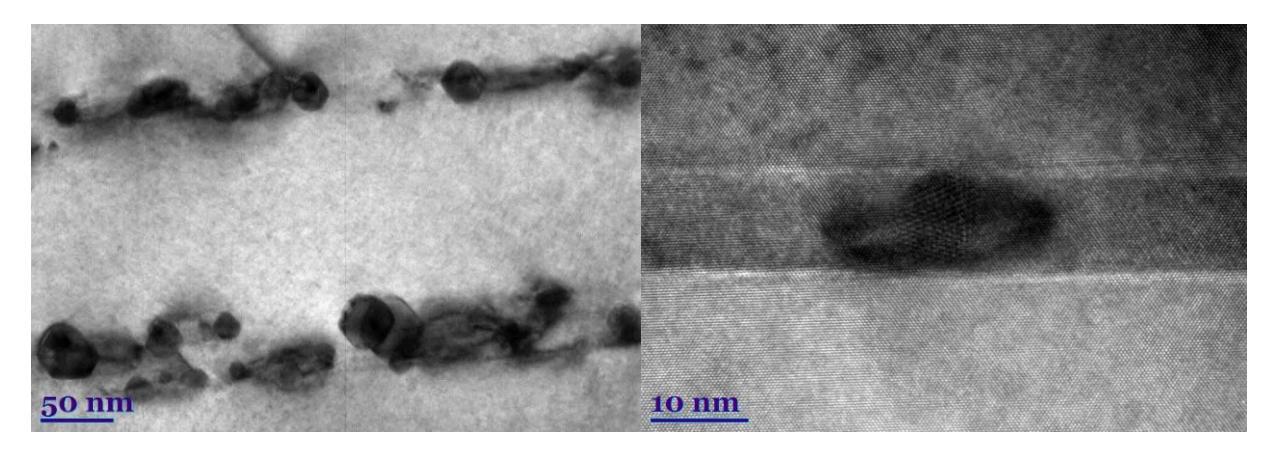
The main goal of this work was to explore new and different from usual Stranski-Krastanov Bi quantum dots formation mechanism employing in-situ bismuth segregation process in Molecular Beam Epitaxy (MBE) reactor via annealing for a short time at higher temperatures under arsenic overpressure conditions. This study would let us to analyze and understand complex quantum effects in AIII-BV-Bi quantum well containing Bi quantum dots and apply them in active media of NIR laser diodes or LEDs. The optimization of growth and in-situ annealing conditions was made in MBE for complex system: ternary GaAsBi and Bi compounds. Main attention in MBE optimization process was concentrated to the search of quantum barriers (which play Bi blocking layer role), GaAsBi well composition (Bi content) and geometry (well thickness and shape). Featured samples were characterized using high resolution transmission electron microscopy, meanwhile all grown quantum structures were examined by photoluminescence measurements.