
Fabry-Perot (FP) resonance is a well-known phenomenon occurring in various fields of physics [1]. It is linked to wave propagation through a transparent material, in this case, dielectric. Due to multiple internal reflections inside the material, propagating waves experience constructive and destructive interference. Those phenomena depend on dielectric thickness and wavelength (frequency). Observing transmission spectra, peak transmittance (constructive interference) occurs at frequencies when inside dielectric slab fits integer number of half-waves. Transmission spectra minimums (destructive interference) happen at frequencies when an odd number of quarter wavelengths match inside the dielectric slab.
Various techniques are proposed to control FP resonance. One of the most popular is using a laser beam to change surface conductivity of substrate to achieve near 95% suppression of resonance [2]. This setup requires the adjustment of the THz beam perpendicularly to the sample together with the laser beam, falling at some angle to it, both having to be focused to the same spot of the sample simultaneously.
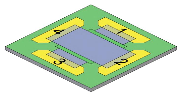
Our work in progress offers a novel way for controlling FP resonance using dielectric substrate covered by graphene capacitor. Its arrangement is shown in Fig. 1. Using atomic layer deposition technology, 60 nm thick HfO2 layer (green) is deposited on a surface of isolating silicon substrate (grey). Image reversal photolithography is applied to form areas for gold contact pads (1-4). Easy transfer graphene layer from Graphenea is placed between contact pads 1-3, later on, Poly(methyl methacrylate) (PMMA) layer covering graphene is removed. Then additional HfO2 layer is placed on the first layer intersection with the second layer (green). Finally, top layer graphene with PMMA is put between pads 2-4.
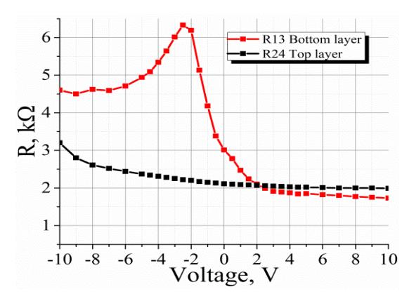
Applying the voltage to the graphene capacitor, the DC measurements are performed by measuring the resistance of each layer. The potential of the top layer determines the voltage polarity in the dependences shown in Fig. 2. One can see that the resistance of the bottom layer demonstrates a sharp resistance spike at -2.5 V that can be attributed to the Dirac point. On the contrary, when the negative voltage is applied to the top layer, it displays a monotonous increase of resistance. The observed difference might be caused by the fact that different layers cover lower and upper graphene sheets. The lower graphene sheet is inserted between HfO2 layers, whereas the upper part of the top sheet is covered by the PMMA layer.
At a voltage corresponding to the Dirac point, the overall conductivity of graphene sheets is the lowest, which suppose the highest transmittance of THz radiation through the silicon plate covered with graphene capacitor. Changing the applied voltage, the conductivity of graphene increases, and in this way, we have demonstrated the modulation of THz radiation.
Since the bottom graphene layer is controlled only, our further research is focused on removing PMMA from the top layer of graphene and changing it with HFO2. We believe that in this way, we shall be able to control the resistance of both layers of the capacitor and increase the efficiency of modulation.