Graphene is a two-dimensional allotrope of carbon consisting of a single layer of atoms. Because of its high charge carrier velocity and extraordinary saturation velocity, graphene field-effect transistors (GFET) have a chance to become serious contenders in the field of terahertz (0.1-10 THz range) electronics [1]. GFET technology is used primarily as THz radiation detectors and has potential applications, such as non-ionizing medical imaging or security screening [1].
GFET technology has seen great improvements during the last decade. The best results for a single transistor so far were published in 2017, reporting the maximum optical responsivity of 74 V/W and the noise equivalent power (NEP) of 130 pW/√Hz at 400 GHz [2]. Despite the achieved promising performance values, GFETs are still heavily outshined by silicon-based detectors [3].
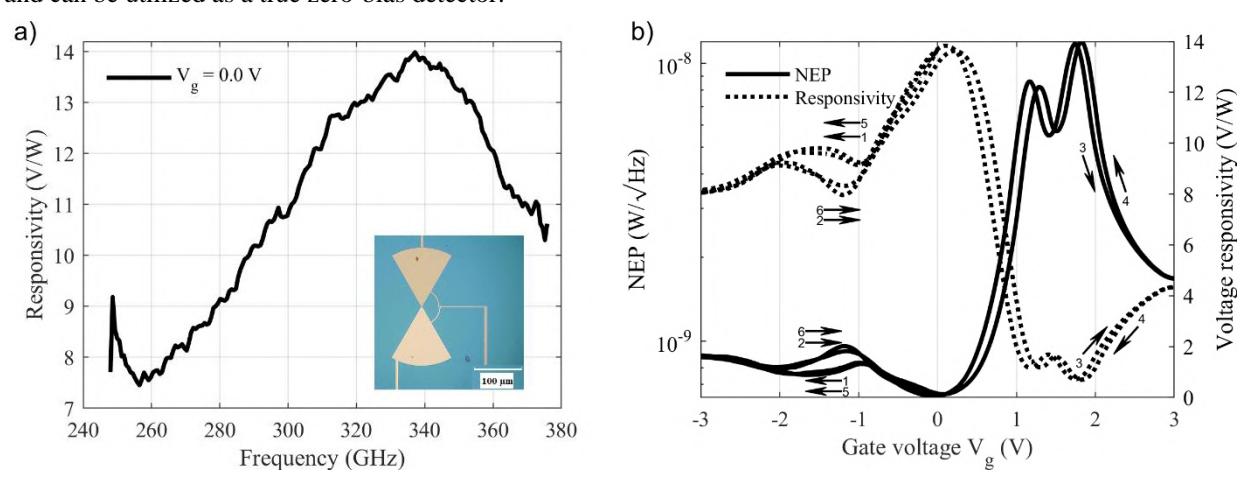
The device used in this study was grown by Chemical Vapor Deposition (CVD) and processed at VTT (Finland). The graphene was transferred onto a SiO2 wafer and formed the field-effect-transistor channel with a channel length of 2 μm. The source and drain contacts are evaporated using Ti/Au. The ALD grown Al2O3 is used as a gate dielectric, another evaporated layer of Ti/Au is used as a gate metal. The source, drain, and gate terminals form a bowtie antenna shown in Fig. 1 a).
The detector's static electrical characteristics were measured using a semiconductor analyzer Keysight B1500A. The frequency multiplier (Virginia Diodes Inc.) and low-noise voltage amplifier were used for the response measurements as a THz radiation source in the 250-380 GHz range. It was calibrated using a Thomas Keating broadband absolute power detector. The optical system employed two 4" parabolic mirrors in a 4-f configuration. A hyper-hemispheric silicon lens (12 mm diameter, 6.8 mm height) was used to focus the THz radiation onto the detector from the substrate side.
Measurements were performed at room temperature (295 K). Fig. 1a presents the measured spectra of optical responsivity. The maximum value of 14 V/W was obtained at 337 GHz frequency. The dependencies of voltage responsivity and NEP on the GFET gate voltage are depicted in Fig. 1b. Both characteristics show a slight hysteresis. It is common in GFET technology and can be suppressed by various methods [4]. More importantly, both the highest responsivity and the lowest NEP of 627 pW/√Hz were observed close to 0 V gate voltage. This means that the detector does not require additional bias and can be utilized as a true zero-bias detector.