Only few percent of bismuth incorporated in GaAs lattice sufficiently reduces the band gap of the material. Large bowing and energy band gap, less sensitive to temperature, makes bismides an attractive material for the applications of optoelectronic devices in infrared range such as light-emitting diodes [1], photodetectors [2], solar cells [3] etc. However, for the optimization of the devices more efficient quantum structure designs should be obtained. Widely used technique to characterize semiconductor structures and track the progress is photoluminescence (PL) measurements.
One of the recently by our group [4] developed quantum structure designs is GaAsBi quantum wells with parabolic AlGaAs barriers (PQW). It was demonstrated that by using this design PL intensity at room temperature was increased by more than 50 times in comparison with conventional rectangular quantum wells. This outcome is related to more efficient carrier trapping into the GaAsBi quantum wells (QW) and carrier localization. It is worth mentioning, that the reproducibility of QW exhibiting enhanced PL using this design is significantly increased.
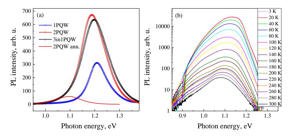
To establish the relationship between technological conditions and optical properties more detailed study of GaAsBi PQW grown by molecular beam epitaxy (MBE) was continued. The latest results will be presented in this work. To explore optical properties temperature-dependent PL measurements were carried out in a temperature range of 3 – 300 K. Moreover, to understand deeper and explain carrier recombination processes excitation-dependent PL experiments were done. The measured spectra revealed the influence of various quantum structure designs to luminescent properties. First, growth parameters (substrate temperature, bismuth content) were varied to increase PL intensity. Then the influence of GaAsBi QW number was investigated by comparing PL spectra of one or two QW with parabolic barrier (1PQW or 2PQW) and three QWs in one parabolic AlGaAs barrier (3in1PQW). The room temperature PL results are presented in Fig. 1 (a). It was demonstrated that thermal annealing, which is traditional way to improve the quality of MBE grown quantum structures, could cause the structural changes as well. The room temperature PL spectra of in situ annealed 2PQW structure is redshifted (see Fig. 1 (a) red line). Moreover, the cross-section transmission electron microscopy images evidenced the formation of Bi nanocrystals during annealing, and increased distortion of the GaAsBi QW layer. Consequently, the PL band of annealed 2PQW structure was assigned to emission from Bi nanocrystals rather than to GaAsBi QW. Wide temperature-dependent PL spectra of annealed 2PQW (Fig. 1 (b)) support that presumption (FWHM = 113 meV at 3 K).