COMPARATIVE STUDY OF WSE2 THIN FILMS SYNTHESIZED VIA PRE-DEPOSITED WO3 AND W PRECURSOR MATERIAL SELENIZATION
Kevon Kadiwala1, Edgars Butanovs1, Andrejs Ogurcovs1, Martins Zubkins1, Boris Polyakov1
1 Institute of Solid State Physics, University of Latvia, Kengaraga street 8, Riga, Latvia, LV-1063
Layered two-dimensional (2D) materials, such as p-type WSe2, are potential key materials in manufacturing of the next generation electronic devices. One of the remaining main challenges is the large area growth of high-quality 2D films. A potential large-scale 2D WSe2 synthesis method is conversion (selenization) of a pre-deposited sacrificial precursor coating, however, its use is still limited mainly due to lack of understanding of the growth mechanisms involved. Here, we have studied and compared properties of thin crystalline WSe2 films, prepared via selenization of sputter-deposited sacrificial WO3 and W films. Surface morphology of the as-grown films was studied using scanning electron microscope complemented with atomic force microscope. Structural and chemical composition was confirmed by X-ray diffraction and micro-Raman spectroscopy, respectively. On-chip photoconductive devices were made using standard photolithography process and their photoresponse was investigated for 405 nm wavelength light. The obtained results give insight into the growth of crystalline WSe2 via sacrificial film selenization.
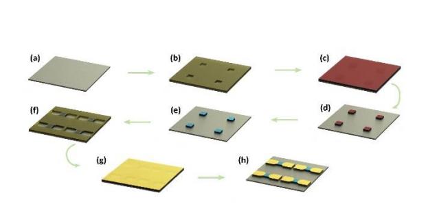
Fig. 1. Schematic of the process of on-chip device fabrication: first SiO2/Si substrate is cleaned using acetone and isopropanol (a), then using standard photolithography process the first mask is made (b) on which precursor material is deposited (c). After first mask lift-off, precursor material film is in desired pattern (d), which is subsequently selenized (e). Afterwards, the second photoresist mask is deposited (f) for the deposition of contact material (Cr ~ 5nm, Ag ~ 95nm, Al ~ 50nm) using thermal evaporation method (g), followed by lift-off to obtain photoconductor device array on chip (h).
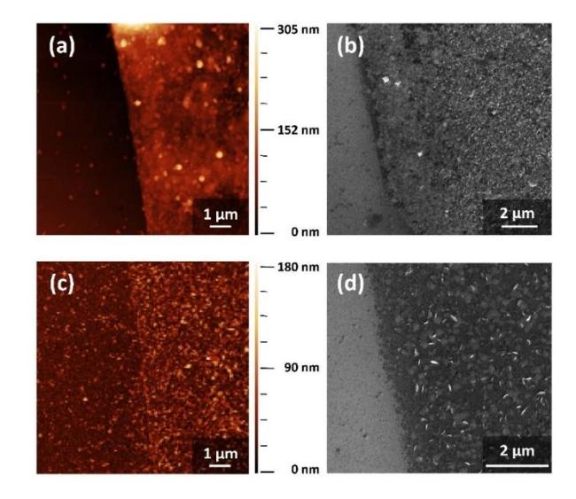
Fig. 2. Atomic force microscope (AFM) Z-drive images of WSe2 films, made from WO3 precursor (a) and from metal W precursor (c) showing the difference between film surfaces, further complimented by SEM images of the same samples in respective order of (b) and (d).
Acknowledgments: The study is financially supported by the Institute of Solid State Physics of the University of Latvia under Student and Young Scientists project.