Waveguide - a structure that confines electromagnetic waves within the material and guides them with minimal loss of energy due to restricted transmission of energy in one direction. The well-known ones are optical fibers, but nowadays as new materials come into play, and having sophisticated fabrication methods waveguides are transferred into a micro-world dimension. One of the new materials is GaN with its' unique properties that make it particularly attractive for the use in waveguiding. GaN excels with its' properties that include wide direct band gap, large transparency window, and high second order nonlinearity (10 pm/V) [1]. GaN waveguides can be used in low loss photonics [2], generation of second harmonic [1], can be fabricated into microrings [2] and microdisks [3]. Latter photonic structures can improve SHG in GaN waveguides as they provide greater power densities [1].
In this work, guiding of 633 nm and 1064 nm wavelength light through planar GaN waveguide grown on a sapphire substrate by metalorganic chemical vapor deposition (MOCVD) using prism coupling technique is investigated.
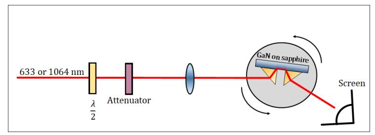
Optical scheme used for waveguiding is depicted in Figure 1. 633 or 1064 nm light is passed through a half-wave plate to control light polarization between transverse electric (TE) and transverse magnetic (TM). Attenuator is placed to lower the energy of 1064 nm pulses. Convex lens is placed that its' focal length is greater than the distance to the prism to avoid potential damage to the prism. Two prisms are made of TiO2 (rutile) and are mounted on a goniometer with custom designed holders. Measurements are performed by selecting single polarization of the light and measuring coupling angles when distinct modes are being guided through GaN. This coupling angle is used in the calculations of effective refractive index of all waveguide modes. The latter is calculated using the following equation:
$$n_e = n_p \sin \left[ A + \sin^{-1} \left( \frac{\sin \theta_i(m)}{n_p} \right) \right]. \tag{1}$$where $n_p$ is prism refractive index, A - prism angle, $\theta_i(m)$ – measured coupling angle for a distinct mode. Thickness of GaN layer was numerically calculated using MATLAB according to the following equation:
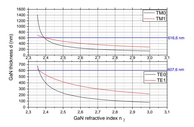
$$\frac{2\pi d(n_2^2 - n_e^2)^{\frac{1}{2}}}{\lambda_0} = m\pi + \Phi_1 + \Phi_3,\tag{2}$$where $n_2$ is refractive index of GaN, $n_e$ – calculated effective index, d – thickness of GaN, $\Phi_n$ – evanescent field phase shifts. Figure 2 shows the calculation results of equation (2). The GaN thickness is obtained from the intersection of the curves.