
Zinc oxide (ZnO) and its properties have gone extensive research since the shortage of short-wavelength optoelectronic devices, transparent electrodes, and materials needed for screen and solar module production [1]. In materials science, it's classified as a semiconductor. When the surface of materials is coated with a ZnO nanoparticle layer, electron transfer improves. This means that ZnO nanostructures have a high surface-to-volume ratio which increases the number of photogenerated charge carriers [2].
Cadmium sulfide (CdS) is a chemical compound profound in its unique size and structure, which can affect its optical and electronic properties. This material can be formed on surfaces using a broad range of methods: vacuum evaporation, spray pyrolysis, or chemical bath deposition (CBD) [3].
In the present work, the deposition of CdS using the chemical bath deposition method on FTO/ZnO was investigated. Thin films were formed on FTO (TEC 10) glass substrates with ZnO nanoparticle layer deposited using the Spin-coating method. Thin films were formed using CdCl2 as a cadmium source, thiourea as a sulfur source, NH4Cl and NH4OH as a complexing agent, and pH control.
UV/Vis analysis was carried out for all samples using ultraviolet light absorption. This analysis was achieved using cleaned FTO glass substrates as standard. Analysis results can be examined in the figure listed below (Fig. 1).
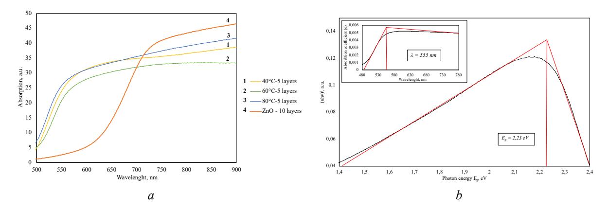
The absorption of various samples can be examined in Fig. 1 (a). ZnO nanoparticles on FTO glass substrates have the best absorption spectra. Samples with CdS had the best absorption when formed at 80°C. Sample with the lowest absorption is when CdS layer is formed at 60°C.
After recording UV/Vis spectra bandgap calculations were carried out, Fig (1, b). This calculation describes electrical properties of materials. bandgap values were calculated using Tauc's relation formula, Eq. (1):
$$\alpha h \nu = A(h_{\nu} - E_g)^n \tag{1}$$The calculated bandgap value of the CdS sample treated at 80°C is Eg = 2,23 eV. The samples absorption starts at 555 nm.