Group III nitride technology has been investigated extensively during the last decades, especially after the creation of the first blue LED. Nitrides have exceptional photonic and electronic properties. For example, gallium nitride (GaN) has a direct band gap which is equal to approximately 3.4 eV [1]. Thus, it can be used as a detector and emitter in the blue region of the visible light spectrum and as a key element in high power transistors. Also, GaN has a more niche application in the biosensing sphere due to outstanding chemical stability and transparency for specific radiation, which enables easy optical readout [2]. For practical application, GaN has to have superb quality and the ability to chemically bond with foreign substrates.
Nitrides are usually grown epitaxially on foreign substrates such as sapphire. The problem of the growth process on foreign substrates is that it deteriorates crystalline quality due to induced stress in the grown material. The stress appears because of the lattice constant and thermal expansion differences between substrate and epilayer. Nearly stress-free GaN can be grown on native substrates or by remote epitaxy via two-dimensional material. In the latter epitaxy, GaN epilayer is formed by its interaction with the GaN substrate through a two-dimensional material such as graphene. The seeding effect of the substrate enables high quality GaN growth through interlayer, while the weak van der Waals interaction facilitates subsequent layer release, reduces grown layer strain and enables the reuse of an expensive substrate [3]. Important aspect of this technology is flexibility of inorganic released layers from graphene due to relatively small thicknesses.
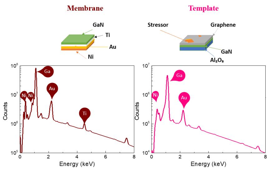
In this work, we investigate the lift-off process of GaN that was grown by remote epitaxy. Before the lift-off process, GaN growth on graphene by MOVPE was studied and afterwards GaN exfoliation was performed by an electrochemically deposited Ni stressor. To enhance adhesion between Ni and the GaN epilayer, Ti and Au metal films were coated by two techniques: electron-beam evaporation or magnetron sputtering. We managed to exfoliate GaN from the growth substrate, on which Ti and Au were deposited by electron beam evaporation. X-ray energy dispersive spectroscopy (EDX) results showed that the GaN film was exfoliated together with stressor metal layers (Fig. 1). After the lift-off procedure, XRD and Raman shift measurements of the exfoliated membrane were conducted. The strain of the released GaN membrane was calculated. Results showed that GaN experienced tensile stress in a direction and compressive stress in c direction.