
Cadmium selenide (CdSe) is a semiconductive material with bulk optical bang gap energy of 1.74 eV, which means it can be excited by low energy, longer wavelength (${\lambda}$ ~ 696 nm) electromagnetic radiation. These properties make it a good candidate material for solar cell applications, as well as high efficiency thin film transistors, photo detectors, light emitting diodes and other optoelectronic devices [1]. Zinc oxide (ZnO) is a semiconductive material with bulk band gap energy of 3.37 eV, good mechanical and thermal stability, optical transparency. Combining the properties offered by CdSe with the properties of ZnO, a functional layer for light energy conversion to electrical energy should be produced, where electrons excited by low energy radiation would be injected into the more electrically conductive ZnO layer and through it – into the outer circuit, reducing the chances of electron and hole recombination [2]. The functional layers were deposited on conductive fluorine doped tin oxide (FTO) coated glass substrates.
The FTO substrates were ultrasonically cleaned in soap solution, distilled water, and ethanol, to remove any impurities from the surface. The ZnO layer was deposited from a suspension of ZnO nanoparticles in ethanol using the spin-coating method. To produce a sufficiently thick layer of ZnO nanoparticles, 10 spin coating operations were performed per substrate, with annealing after each deposition. CdSe layers were deposited using two methods: successive ionic layer adsorption and reaction (SILAR) method, chemical bath deposition (CBD) method and combinations of the two.
For the SILAR method, cadmium acetate (Cd(CH3COO)2) solution was used as the cation source and sodium selenosulfate (Na2SeSO3) as the anion source. The CdSe thin film is formed by performing 30 SILAR cycles with annealing after every 5th cycle. For the CBD method, the substrates were treated in diluted reaction mixture of Cd(CH3COO)2, Na2SeSO3 and a chelating agent for reaction rate control for 30 minutes. The CdSe thin film is formed by performing 4 CBD reactions, with annealing after each one. Two variations of combining CBD and SILAR methods were also investigated: one variation had CdSe thin film deposited with 15 SILAR cycles first and 2 CBD reactions second, the other variation had the thin film deposited with 2 CBD reactions first and 15 SILAR cycles second.
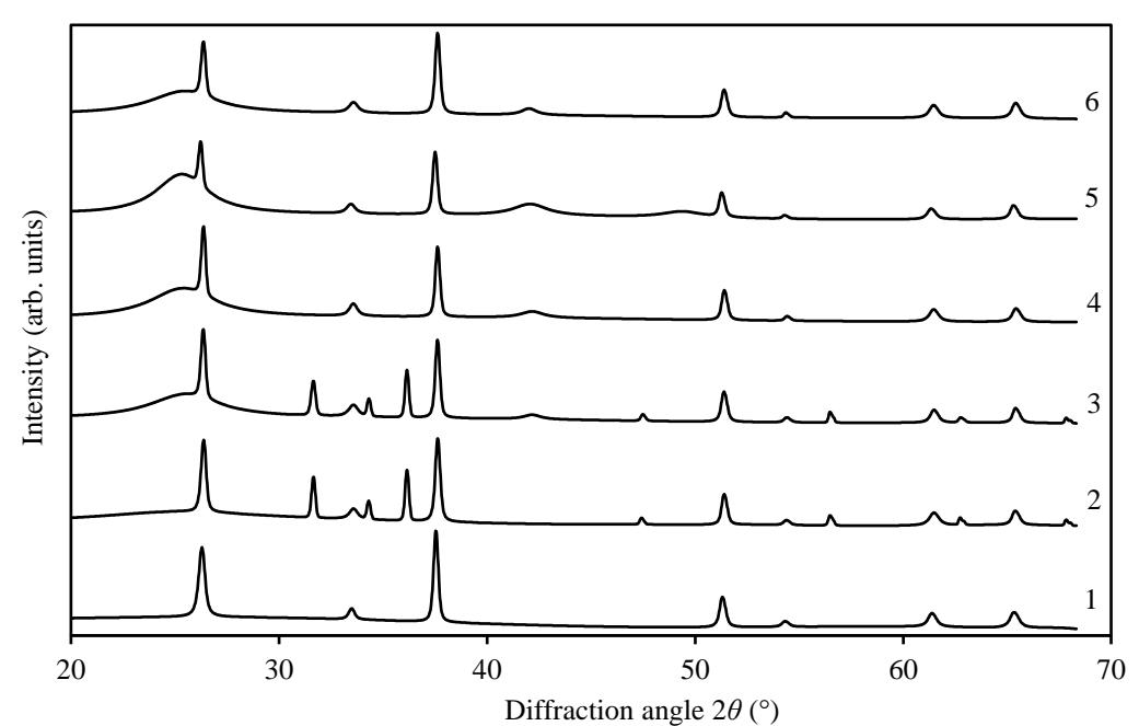
The X-ray diffraction patterns show that diffraction peaks that appeared with the deposition of ZnO nanoparticles disappear in every CdSe sample, where CBD method was used, but remain in the sample where only SILAR was used.