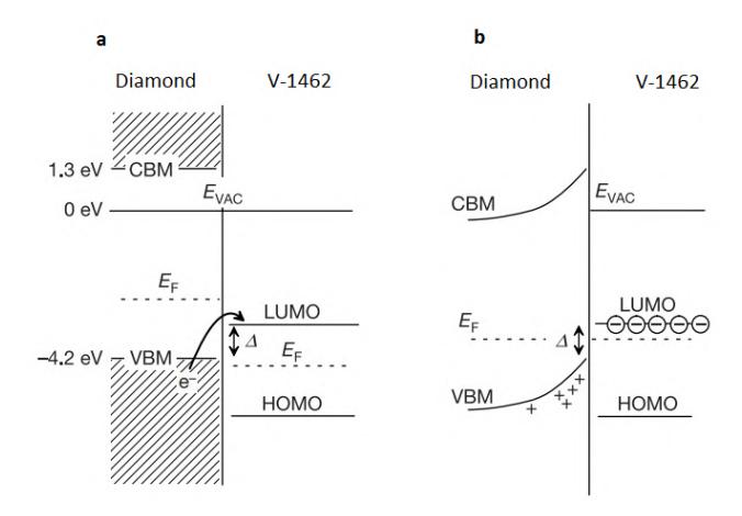
Focus of the researchers on diamond electronics has been intensified, when it was demonstrated that C-H bonds are formed on diamond surface after treatment with hydrogen plasma. This treatment creates conductive surface known as H-terminated surface. H-terminated surface creates two dimensional hole gas (2DHG) with carriers mobility of 30 - 200 (cm2/Vs) and carrier density of the order of 1013 (cm-2) [1]. A number of devices, based on this principle, already have been produced. However, the 2DHG surface is not stable chemically and conductivity depends on the environment.
When diamond is terminated by hydrogen, C-H bond at the terminated surface creates a dipole layer that induces a negative electron affinity $\chi$. The transfer of electrons from the diamond valence band into the accepting state of an appropriate adsorbate layer on the diamond surface gives rise to subsurface hole accumulation and p-type surface conductivity [2]. This phenomena is also known as “surface transfer doping“ and it is not limited to just atmospheric adsorbate molecules.
We demonstrate the influence of newly synthesized organic materials on electrical properties of H-terminated diamond surface. The charge transfer from diamond to organic acceptor layer is ensured by the selection of organic materials with as low as -3.52 eV and -4.48 eV LUMO (lowest unoccupied molecular orbit) energetic levels (Fig. 1).