Over the last decade hybrid metal-halide perovskites have attracted huge interest in the semiconductor and optoelectronics science community. A combination of easy and cheap synthesis from solution and excellent optoelectronic properties makes these materials excellent for devices like solar cells, LED's, photodetectors, transistors and many more [1]. However, many uncertainties concerning the stability of perovskite devices under working conditions remain.
In our work we seek to measure and identify processes causing perovskite device instability under applied electric field. Using florescence microscopy, we report photoluminescence (PL) properties of CH3NH3PbI3 (MAPI) thin films deposited on interdigitated electrodes under the applied electric field. Additionally, for electric-field mapping inside the perovskite film an electric field-induced second harmonic (EFISH) microscopy technique was performed.
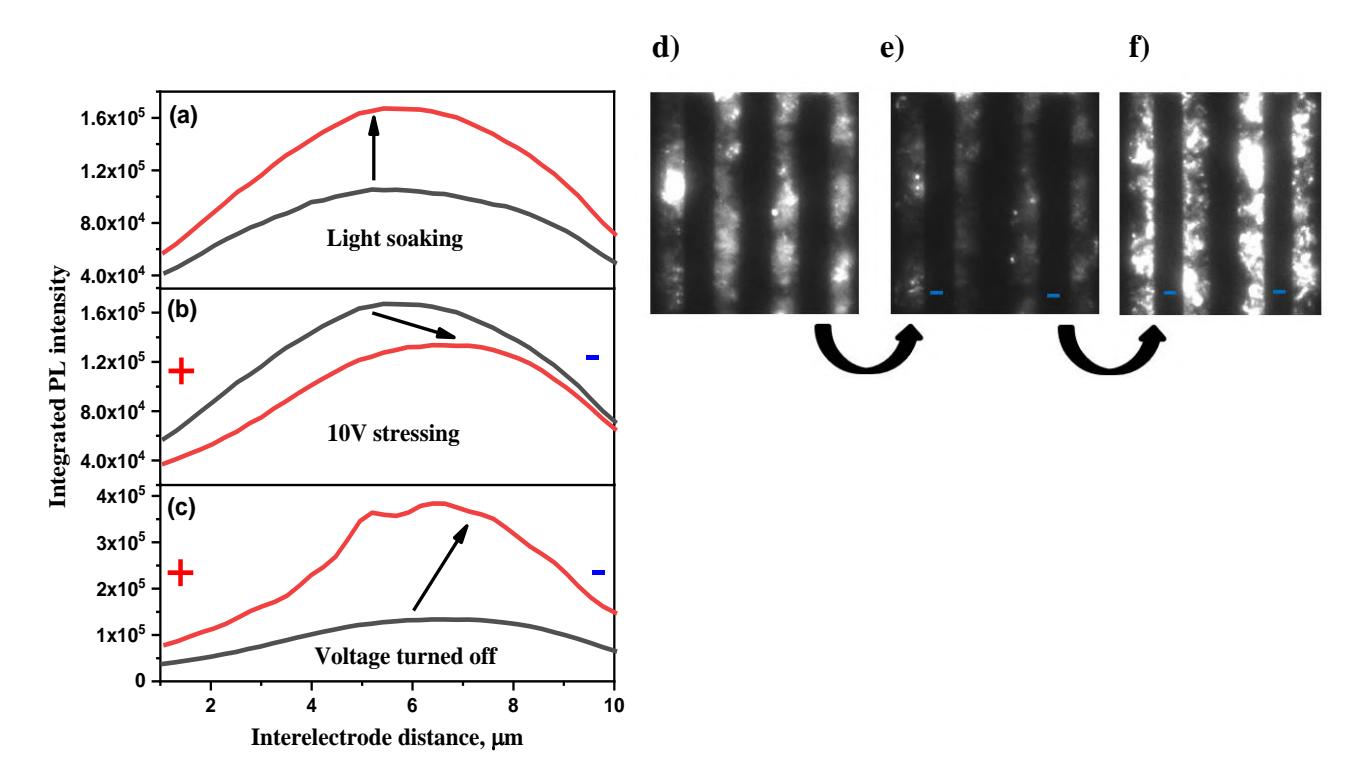
Three main PL dynamic steps were observed: a dark PL front moving from the positive electrode side throughout the perovskite film at the start of voltage stressing, a change of homogenous PL distribution to many bright blinking spots in a dark background and finally, after the voltage is turned off an increase of PL near the negative electrode.
Combining these results with EFISH microscopy we propose a model explaining such PL dynamics. We suggest that two types of PL quenching defects become active under applied electric field. The first one is caused by negatively charged ionic interstitials drifting throughout the perovskite film and causing a polarity-dependant PL quenching which is seen at the start of voltage stressing and after voltage termination. The second quenchers are immobile shallow ionic traps that form deep lying PL quenching states after interaction with injected holes.