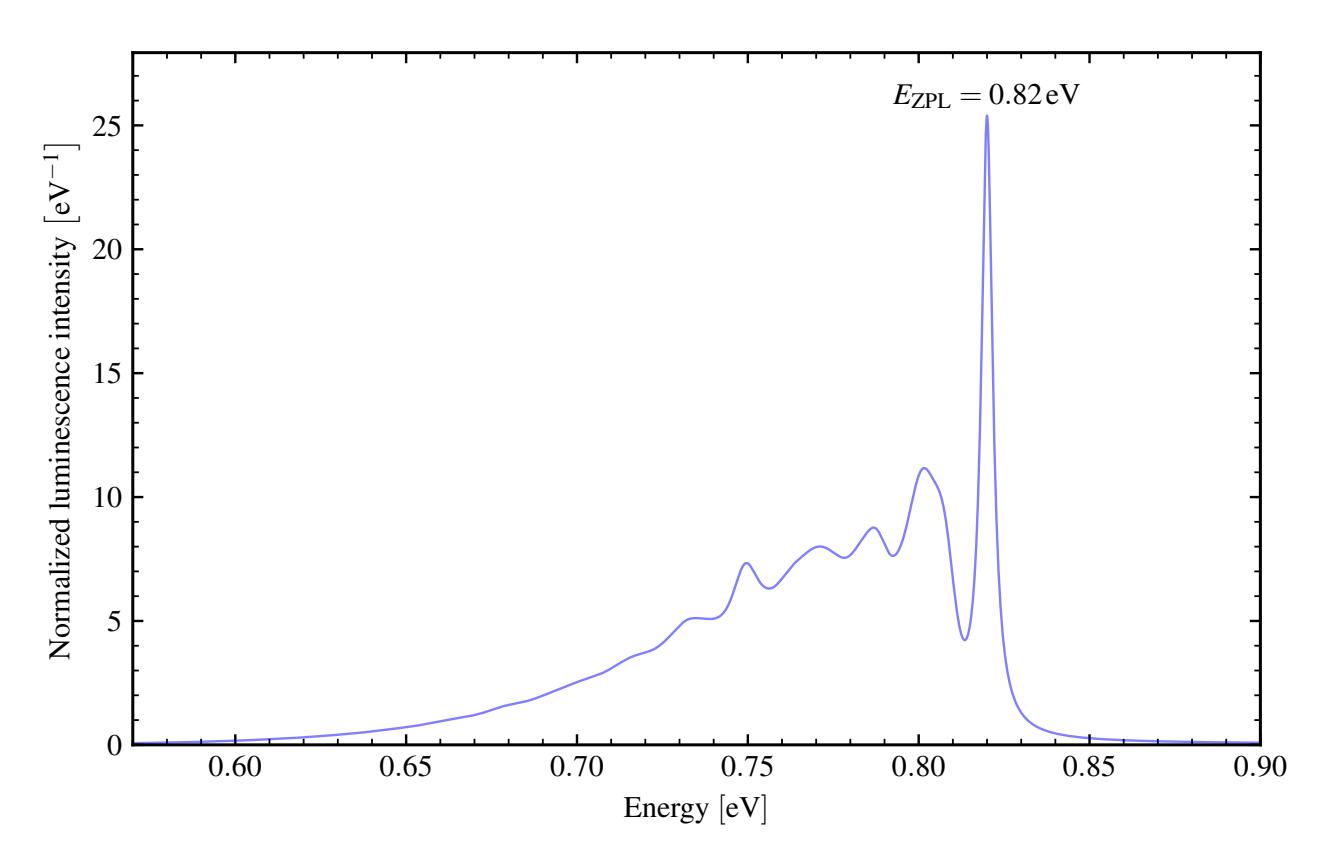
In recent years quantum technologies have been at the forefront of scientific interest due to a vast array of possible applications in sensing, communications, and computing. Given its history of commercial and practical success as an essential part of solid-state devices, silicon seems to be a rational choice as a host material for future quantum technologies. Of particular interest are optically-active single point defects which could be used for long-distance exchange of information [1]. The so called G-center, thought to be composed of an interstitial-substitutional carbon pair ($C_iC_s$) in silicon, is one of such defects [2, 3, 4]. It emits light at telecom wavelengths of 1280 nm (0.97 eV) and is thus a suitable candidate for a telecom-range single-photon source [5].
In this work, we present a theoretical analysis of the luminescence lineshape of the $C_iC_s$ defect in silicon. We performed first principles density functional theory (DFT) calculations with a semilocal functional based on the generalized gradient approximation (GGA), in particular the Perdew–Burke–Ernzerhof (PBE) variant. Our results indicate a zero-phonon line (ZPL) energy of 0.82 eV, which is comparable to the experimental value of 0.97 eV. The Debye–Waller factor $w_{ZPL}$ (the weight of the ZPL) and the Huang–Rhys factor S (the average number of phonons emitted during an optical transition) are calculated to be 12% and 2.08, respectively. The calculated lineshape agrees with the experimental results for the G-center closely. This reinforces the conclusion that the G-center is the $C_iC_s$ pair.