Bloch surface waves (BSW) are waves propagating along the surface of periodic multilayer structure – one-dimensional photonic crystal (PC). The BSW could be applied in different fields of photonics, for example in photonic integrated circuits. BSW have some advantages over the surface plasmon polaritons (SPP), which had been widely studied in recent years. Firstly, the BSW attenuate slowly than the SPP and have much longer propagation length. The characteristic propagation length of SPP is about 10-100 μm [1], while the propagation length of the BSW in experiments reaches the value of 500 μm [2]. Secondly, the excitation conditions of SPP are determined by the type of metal, while the BSW could be excited in the wide wavelength range. It could be done by selecting materials and thickness of layers of the PC. The possibility of making the dielectric stripe waveguide on the surface of the PC was demonstrated in the paper [3]. However, the photonic circuits such as splitters, interferometers and others haven't been fabricated on the surface of the PC yet. In this paper we would like to present the waveguide structures for the BSW fabricated on the surface of the PC by the method of two-photon lithography (TPL) - the method of direct laser writing based on the phenomenon of two-photon absorption (TPA), which causes the reaction of polymerization of special photosensitive material - photoresist.
By using the TPL scientists can achieve resolution beyond the diffraction limit: the size of voxel (3D pixel) could be less than 100 nm [4]. The TPL is also effective for fabricating planar structures, because this method allows scientists to make many structures in one exposure session. Moreover, if structures are being made in regime of overexposure (when the size of voxel is larger than the thickness of polymer film), it is easy to control shape and thickness of structures. This advantage of the TPL is very important for fabricating waveguide structures for the BSW, because BSW are very sensitive to the thickness of the top layer or the waveguide structure.
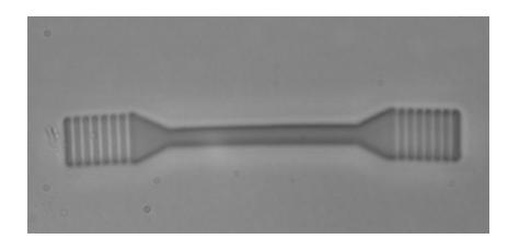
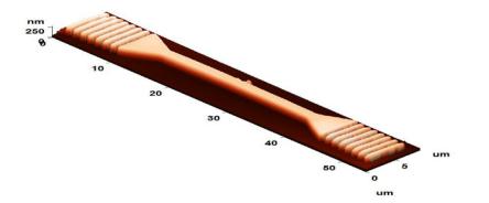
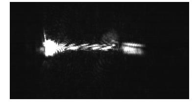
In our work we use photoresist SU-8 2015 for fabrication structures by the TPL. The standard procedure allows obtaining films with thickness about 15 μm. For effective excitation of the BSW in our the PC the films with thickness of 200-400 nm are required. So, we decided to dilute photoresist with developer MR DEV 600. Solutions with different concentrations of SU-8 2015 were made. By using the solution with concentration 14,3% we achieved suitable film thickness and fabricated the waveguide structure, which supports excitation and propagation of the BSW. The Fig.1 and Fig.2 show one of the structures fabricated by our group. It is a waveguide for the BSW (20 μm long and 2 μm thick) with diffraction gratings and concentrating triangles. Fig 3. shows propagation of light in the waveguide structure. Furthermore, we have made other types of structures, such as interferometers and splitters and achieved resolution about 200 nm.