This work discusses the development of wide band gap semiconductor radiation detector formation method. Gallium nitride (GaN) was chosen as a suitable material for radiation damage resistant detector. The development of semiconductor detector with a higher radiation damage resistance is very important for many scientific applications, which can't rely on ordinary silicon detectors as they would decay faster than in few years. For example open space radiation can damage silicon detectors which are equipped in orbiting X-ray telescopes. GaN's wide band gap should result in detector with lower leakage currents than an equivalent Si detector. A further possible advantage of using GaN as a detector is that its displacement energy may be larger than Si resulting in it being more intrinsically resistant to radiation damage. In general there are several possible geometries in which semiconductor detectors could be made: p-n, Schottky or capacitor structures. It was decided to make capacitor detector, because the difficulties to growth p-doped GaN and complexity of ohmic contacts formation.
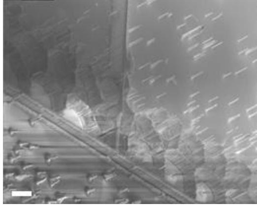
In order to fulfill detector in such geometry, extremely thick (~20 μm) GaN wafers are needed, which in this case were grown on a sapphire substrate using metalorganic chemical vapor deposition (MOCVD) reactor. Desirable aspect ratio of capacitor type mesa device is 1:10 or more and it could not been achieved using ordinary photolithography method. Instead femtosecond laser fabricated glass shadow masks were used for GaN mesa formation by dry etching process. However it resulted in formation of dry-etch resistant polymer structures around the inner features of the mask (see Fig. 1). It was shown that ex-situ sample treatment with 0.5 % KOH solution after every etching process effectively etch the polymer. Thus, polymer-free mesa structure is demonstrated, suitable for capacitor type GaN detector formation.