
Thin films of Cu2ZnSnSe4 (CZTSe) contains a low-cost non-toxic elements which are abundant in the Earth's crust and therefore are promising absorber semiconductor material for photovoltaic cells. The natural p-type doping of CZTSe is caused by intrinsic defects and therefore the determination of a nature such defects can help to accelerate progress in the solar cells performance. In the present study the photoluminescence (PL) and photoluminescence excitation (PLE) spectra were investigated at low temperature ~ 4.2 K to determine the nature of intrinsic defects and the mechanisms of a radiative recombination in CZTSe absorber layers. CZTSe thin films were prepared by selenisation of metallic Cu, Zn and Sn precursor deposited by magnetron sputtering on to Mo-coated glass substrates. The surface morphology and cross-section analyses were carry out by scanning electron microscopy (SEM). These experiments show a gradual increase of the grain size with the selenisation temperature rise in range of 450 – 550 °C. X-ray diffraction measurements were made by using a Siemens D-5000 diffractometer. These investigations are indicated on the formation of tetragonal CZTSe polycrystalline films for all range of selenisation temperatures. As an example the PL and PLE spectra taken at 4.2 K for the three samples (film 1 and film 2 ~ 500 °C, film 3 ~ 450 °C) at 532 nm laser excitation with power density of about ~ 0.01 W.cm-2 are shown in Fig. 1. In all the three case the PL bands at 0.77, 0.91 and 0.92 eV for films 1, 2 and 3, respectively, shows significant shifts to higher energies with increasing laser power.
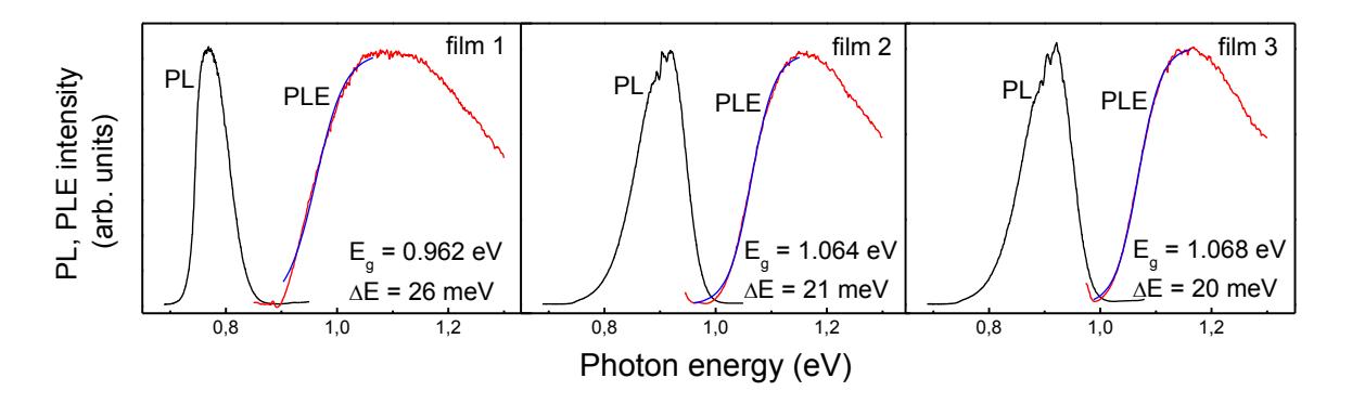
The blue shift increases from 11 to 14 meV per decade of excitation power as the selenisation temperature rises from 450 °C to 500 °C. Such j-shift PL bands with their asymmetric shape at 4.2 K imply that the radiative recombination is related with band to-tail optical transition that comprises free electrons and holes that are localized in the valence band tails formed by randomly distributed potential fluctuations in crystal lattice of CZTSe. The bandgap energy $E_g$ of the thin films was determinate from PLE spectra, Fig. 1. The PLE spectra show broadening which suggests the presence of sub-bandgap absorption states associated with band tails. To take into account such broadening the low energy sides of the PLE spectra, representing absorptance $\alpha(E)$, are fitted with sigmoidal function: $\alpha(E) = \alpha_0/(1 + \exp(E_g – E)/\Delta E)$, where $E_g$ is the bandgap, E is excitation energy at which the intensity of emission is recorded and $\Delta E$ is a broadening parameter (energy steepness). The Cu and Zn atoms in the kesterite structure of CZTSe can be either ordered or randomized on the cation sub-lattice. Such an ordering increases $E_g$ and spectral energy of PL bands, Fig. 1. The change in the optical parameters is consistent with a reduction of the CuZn and ZnCu-VCu as well as with increasing ordering of Cu and Zn atoms. It is proposed that the observed change of $E_g$ are associated with the Cu–Zn ordering and are defined by the change in [Cu]/[Zn+Sn] ratio. This results demonstrate that [Cu]/[Zn+Sn] ratio can be used to control electronic characteristics of CZTSe thin films such as $E_g$ and $\Delta E$ as well as solar cells fabricated using these films.