
The fabrication of nanowire (NW) devices on alien substrates is necessary for applications such as flexible electronics, conformable sensors, and transparent solar cells. Although NWs have been fabricated on plastic and glass by lithographic methods, but these are limited by its temperature and the property of the alien substrate [1].
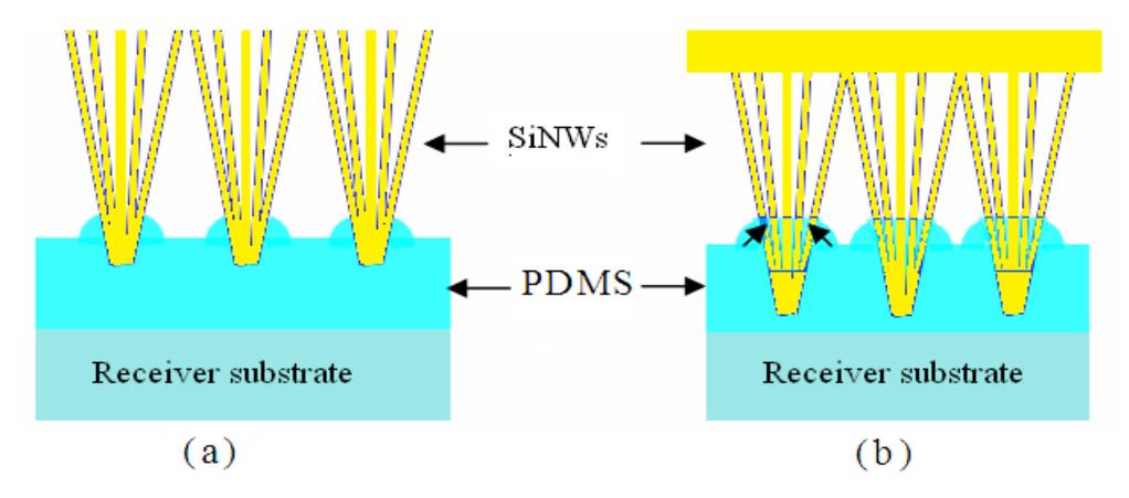
Here we demonstrate the method of relocation of aligned single crystal silicon nanowires (SiNWs) to alien substrate. The methods of transferring basically rely on the differences in adhesion of NWs, metal films, and devices from weakly adhesive donor substrates to more strongly adhesive receiver substrates. The Fig. 1(a) shows Metal assisted chemical etching (MACE) method used to fabricate vertically aligned SiNWs on Si substrates [2]. To detach SiNWs from Si substrates, the roots of the Si NWs were etched and became fragile by controlling direction of metal-assisted etching. Thus, every SiNW on the Si substrate can be easily transferred to alien substrates Fig. 1(b).
The transmission coefficient below 10 % at a wide bandwidth, 400-1100 nm, was found in the transferred SiNWs and the alignment of the transferred nanowires was found to be almost same to the original. This high dense aligned SiNWs are promising for future photovoltaic applications [3]. At low temperature process, it enables a large variety of alien substrates to use.