
Lattice-matched GaInAs/InP system is widely investigated and applied in optoelectronics for telecommunications and near-infrared applications up to ~1.7 µm wavelengths. Theoretically, it is possible to reach ~3.5 µm spectral range, but a development of high performance devices is limited by relatively large lattice-mismatch between GalnAs compound with high In content and InP substrate. The more prospective alternative for GaInAs could be GaInAsBi compound. Even low incorporation of Bi can considerably reduce bandgap ($E_g$). Proper selection of In and Bi content allows to grow latticed-matched GaInAsBi/InP systems working up to 6 µm [1].
The aim of this work was to growth quaternary GaInAsBi layers on semi-insulating InP:Fe (100) substrates using molecular-beam-epitaxy (MBE) reactor and characterize them. For characterization of crystallographic and optical properties of GaInAsBi layers, structural (HR-XRD, AFM, TEM) and optical (photoluminescence and transmittance) methods were selected.
Initially, GaInAs buffer layers for substrate smoothing were grown. The optimal In/Ga flux ratio for GaInAs layers lattice-matched to InP substrate was chosen. Afterwards GaInAsBi layers with same and smaller (to reduce strain caused by bismuth incorporation) In/Ga flux ratio and Bi/Ga flux ratio from 0,13 to 0,35 were grown on a buffer layer. Figure 1 shows the rocking curve dependence on Bi/Ga flux ratio. It is evidence that larger Bi flux shifts the peak related to the GaInAsBi layer to smaller angles keeping In/Ga flux ratio constant.
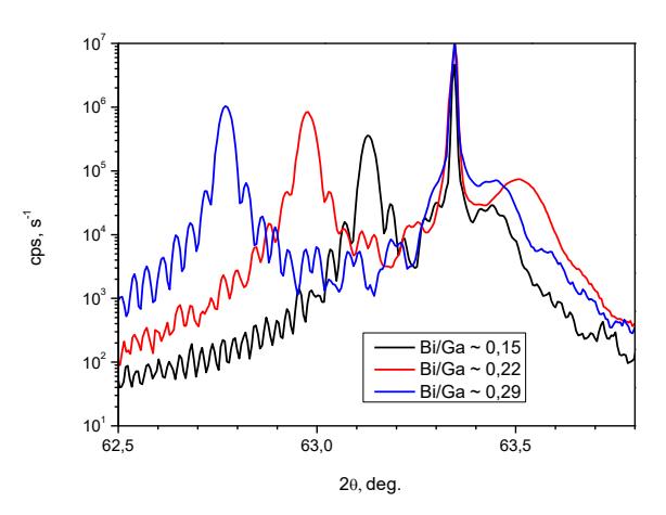
To avoid lattice distortion due to larger Bi atoms incorporation into InGaAs lattice, In concentration in buffer layer was increased to obtain the same lattice constant of buffer and bismide layer. AFM investigation revealed no significant difference in surface roughness for layers with different buffer composition. The elemental composition was optimized for lower $E_g$ value, what was demonstrated in photoluminescence spectra, the emission peak was shifted to 0.52 eV (~2.4 µm).
GaInAsBi layers were successfully grown by MBE on InP substrates. The room temperature luminescence was observed. $E_g$ values as small as 0.52 eV demonstrate that these layers are suitable to apply for mid-IR optoelectronics devices. Our future plans are to extend the bismide operation range by minimizing the lattice mismatch and shifting the characteristic emission to longer wavelengths.