
Size reduction of semiconductor devices has led to increasing role of dopants position in a working area of a device. The abiliby to control accurately the location of dopant atoms allows to create devices with one or several donor atoms, which functionality is based on electron wave function relocation [1]. An example of such devices is a spin-based quantum computer proposal [2]. The effect of external electric field on donor electron has been studied earlier in cases of a thin disc-shaped gate [3] and uniform electric field [4]. However, these cases do not represent real device geometries.
In this work, we consider the following system: the area $z > 0$ is filled with a semiconductor, a donor is positioned at a distance $z_0$ from a semiconductor surface. External electric field is applied by the gate, situated on the plane $z = 0$. The donor is centered with respect to the gate. Within the effective mass approach, donor electron energy $E$ and wave function $\Psi$ in semiconductor are described by the stationary Schrödinger equation
$$\left(-\nabla^2 + \hat{V}_G^{(i)} - \frac{2}{\sqrt{x^2 + y^2 + (z - z_0)^2}}\right) \Psi = E\Psi, \quad z > 0, \quad i = \{A_1, A_2, B, C\}\tag{1}$$$$\Psi\big|_{z=0} = 0; \quad \Psi \to 0 \quad \text{as} \quad |\vec{r}| \to \infty.\tag{2}$$where $\hat{V}_G^{(i)}$ is external electric field potential induced by the gate. Several types of the controlling gates have been considered:
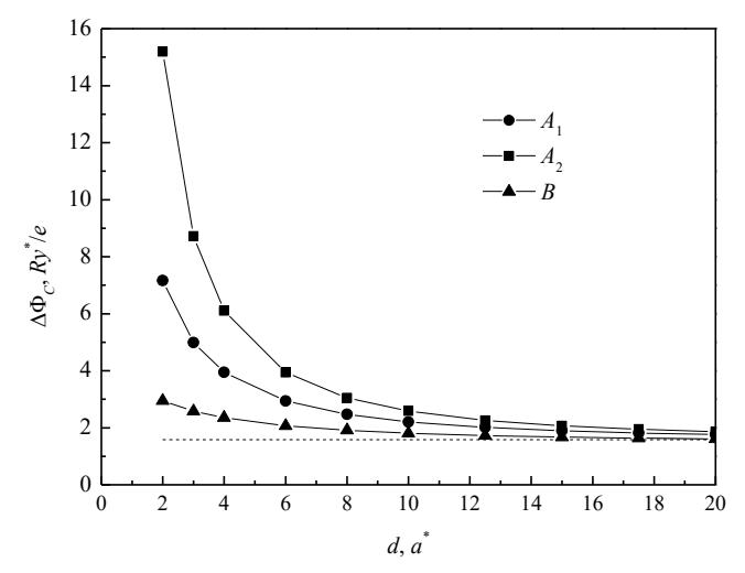
1) A1 - the electric field is applied by a thin disc of diameter d, situated at a semiconductor-insulator interface;
2) A2 – the electric field is applied by a disc of diameter d, surrounded by a grounded shield;
3) B- the gate has a form of unbounded thin strip of width d;
4) C- the external electric field is uniform.
Expressions for $\hat{V}_G^{(i)}$ in cases A1 and A2 are given in [4], in case B - in [5].
The problem (1) – (2) has been studied numerically using the finite element method (FEM) and the variational method. Two main characteristics of the system functionality have been studied:a critical potential difference between the gate and the donor position (ΔΦC) and an exchange interaction between electrons bounded to neighbouring donors or quantum dots.
The value of ΔΦC has been calculated as the minimum point of the difference between first excited and ground state energies. The dependence of ΔΦC on d is shown in Fig. 1. It has been found that the value of z0 practically does not affect ΔΦC in cases A1 and A2 (ΔΦC varies by no more than 2% when z0 changes from 8a* to 16a*) and has more influence in cases B and C (for the uniform electric field the change of ΔΦC reaches 20%).
As the exchange coupling between two electrons is essential for qubit entanglement, we have also investigated the effect of geometrical parameters on the overlap integral and the exchange energy, which has been calculated using Heitler-London method.
The results of this work allow to select the most efficient form of the controlling gate used in few-electron nanoelectronic devices.