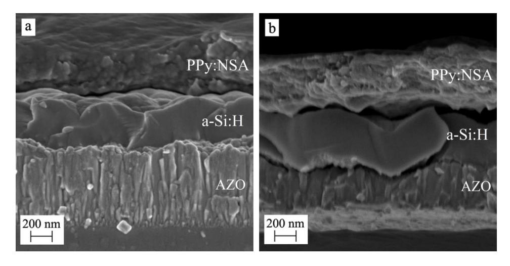
In this study, a number of hybrid solar cells (polypyrrole (PPy)/i-a-Si:H/n-a-Si:H/AZO/glass) with an n-i-p structure has been prepared and characterized electrochemically. Hydrogenated amorphous silicon (a-Si:H) was used as a substrate with n-doped (n-a-Si:H) and intrinsic (i-a-Si:H) layers, which acted as a charge separation and photo-absorber layer, respectively. Doped PPy was deposited onto the i-a-Si:H layer using selective photo-assisted electrodeposition (ED) technique under either a red laser illumination or Xe lamp illumination in a standard three-electrode cell. ED was held at room temperature in an aqueous solution containing 1-naphtalene sulfonate or polystyrene sulfonate doping agents for PPy at low potential values ranging from 300 mV to 500 mV vs. SCE. At these potential values, PPy covers selectively only photo-activated area of i-a-Si:H photoabsorber layer. For the first time, photo-assisted ED of PPy onto a-Si:H surface was applied in order to create a working hybrid solar cell with such n-i-p structure. The efficiency of the photo-assisted ED technique for producing of conductive uniform PPy layers onto the i-a-Si:H photoabsorber is confirmed. The overall photoconversion efficiency of the best prepared hybrid solar cells was about 2.9% and comparable for different doping agents for PPy and illumination conditions for ED process.