
Graphene has attracted a lot of attention as a novel material, which could replace silicon in semiconductor applications [1]. It is expected to demonstrate exceptional electrical conductivity, absorption, luminescence, etc. [2]. Practical applications of graphene are still limited mainly because of the lithography processes. Femtosecond laser ablation is a non-thermal process in its nature, thus this technique is capable to fabricate high quality structures and has a potential in graphene patterning applications [3]. In this work, we present graphene ablation using various femtosecond laser parameters to find the optimal ablation conditions. Graphene was prepared by atmospheric pressure chemical vapour deposition on copper foil from decane precursor and transferred on Si/SiO2 substrates.
Graphene was processed employing Pharos femtosecond laser (Light Conversion) and micromachining work station FemtoLAB (Altechna R&D). Laser affected squares of $70 \times 70 \ \mu m$ were used for micro Raman spectroscopy (inVia, Renishaw). The 1030 nm wavelength beam was scanned using galvo-scanner system (ScanLab). The 200 kHz repetition rate was selected for this task. The mean power was changed from 3.2 mW to 35.3 mW while the gaps between fabricated lines were varied from 1 μm to 3.8 μm using constant frequency mode with 100 mm/s fabrication speed.
Raman measurements were performed with laser wavelength of 532 nm and 45 mW power employing x50 objective. Spectrum range from 600 cm-1 to 3200 cm-1 was used for analysis in order to avoid saturation of spectra by silicon peak at 520 cm-1. Measurements were repeated three times. Raman spectra acquired from pristine and under two different conditions laser processed graphene are depicted in Fig. 1.
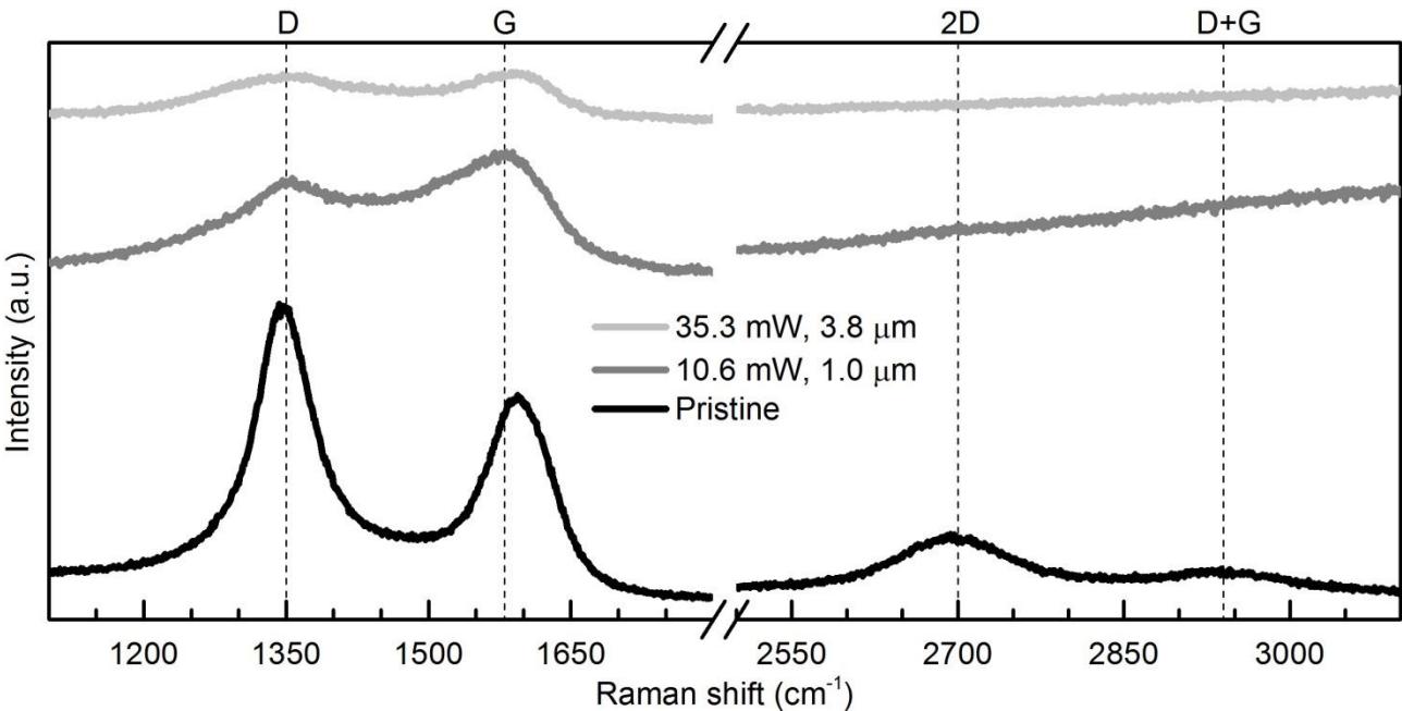
It was demonstrated that femtosecond laser ablation can be used as a single step lithography tool for processing of graphene. Raman spectroscopy was used to define the ablation threshold and determine the composition changes on the laser processed graphene. The intensities of D and G peaks change depending on laser ablation parameters. However, it is not totally clear, if 2D and D+G peaks disappear or they are overrun by background signal. They are no longer visible after ablation with 10.6 mW laser power and 1.0 μm hatch gap.