
High Resolution Transmission electron microscopy (HRTEM) is the premier tool for understanding the internal microstructure of materials at the nanometer level. It allows one to obtain real-space images of materials with resolutions on the order of a few tenths to a few nanometers, depending on the imaging conditions, and simultaneously obtain diffraction information from specific regions in the images (e.g., nanoparticles)[1]. Variations in the intensity of electron scattering across a thin specimen can be used to image strain fields, defects such as dislocations and second-phase particles, and even atomic columns in materials under certain imaging conditions. In addition, the high-energy electrons (in Tecnai G2 F20 - 200 keV of kinetic energy) in TEM cause electronic excitations of the atoms in the specimen, thus allowing spectroscopic techniques make use of these excitations by incorporating suitable detector into the transmission electron microscope, such as energy-dispersive x-ray spectroscopy Nanometer-scale chemical compositional analysis can be performed by using a focused electron probe. Spatial distribution of elements can be obtained by scanning the probe over the specimen.
In this work, various TEM techniques are presented that were used for analysis of layered structures of GaAs, GaN and LSMO. Samples were prepared using Dual Beam Scanning microscope Helios Nanolab650. TEM images were obtained using 200kV TEM microscope FEI Tecnai G2 F20 equiped with Scaning module and High angle annular dark field detector for STEM mode, energy dispersive X-ray spectrometer EDAX, 11MPix ORIUS SC1000B (Gatan) CCD camera, single and double tilt specimen holders.
TEM allows making elemental analysis using energy dispersive X-ray spectrometer to be done in a very minute regions of sample. Features less than 10nm were be identified both by elemental and phase composition (fig. 1), compared with EDS resolution of SEM of around 1µm and XRD resolution of around 1mm.
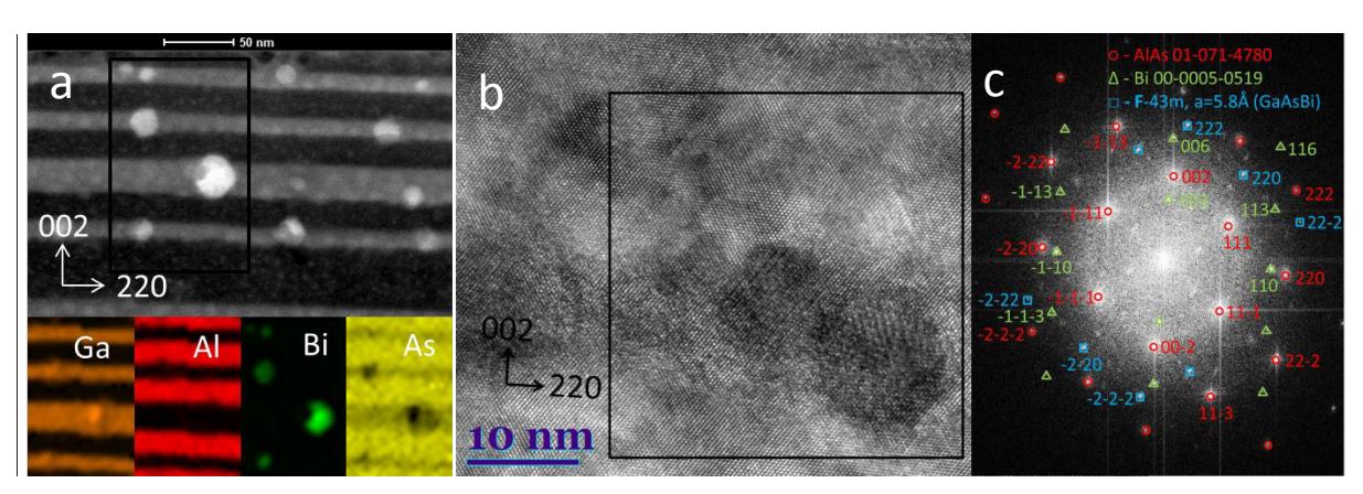
Other samples, such as GaN or LSMO thin layers were also investigated using Dark-Field imaging technique, that allowed analysis of polycrystalline films or crystal defects. Using this technique, image is formed from selected diffraction reflex only, so only desired orientation features are visible, while other parts of the sample remains in the dark-field.