
The resistance of the contacts between graphene and metals is frequently the limiting factor in development of the graphene based electronic elements for practical applications. The characteristics of the contacts depend on the fundamental mechanisms of an interaction in the interface commonly identified as physisorbtion and chemisorbtion of metals on graphene. For the physisorbed metals, the outer shell s orbital interacts with graphene π orbital that results in weak interaction. For the chemisorbed metals the d orbital strongly interacts with graphene π orbital. The interaction mechanism allows to predict the minimal contact resistance [1]. However, there is still a great challenge to make the predictable contact.
This work focuses on the contact technology between graphene and metals, namely nickel and gold. An influence of thermal treatment on the resistance is studied. The contact resistance was measured for the samples adapted to the circular transfer length method (CTLM) [2]. For the contacts, the metal films were deposited by magnetron sputtering and shaped by photolithography. Then, a CVD grown graphene sheet was lifted from a copper foil and placed on the shaped metal film. We developed a wet transfer process for this. Polymethyl methacrylate (PMMA) was spin coated on the graphene. The copper substrtae was removed by etching and the PMMA with graphene was placed on the test sample. Then the PMMA was dissolved in chloroform. The I-V characteristics and the Raman spectra were obtained for the samples before and after annealing at 580 K. An influence of the annealing time on the experimental data was studied.
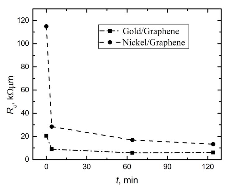
Extracted Gold/Graphene contact resistance before annealing was 20.63 kΩμm and after thermal treatment was reduced to 5.8 kΩμm. The largest reduction of contact resistance (80 % of total reduction) was achieved through first 4 minutes of thermal treatment. Nickel/Graphene resistance before annealing was 114.9 kΩμm and after annealing was reduced to 13.3 kΩμm. Contact resistance reduction of Nickel/Graphene structures was similar as Gold/Graphene. The largest drop of contact resistance (85 % of total reduction) was achieved through first 4 minutes also. Contact resistance dependence on annealing time for both structures presented in figure 1. Raman spectra of graphene on nickel showed, that after 4 minutes annealing nickel carbide begins to form. Wider investigation showed that carbide can be formed due to supporting polymer residues and contamination from photolithography resist during contact annealing.