
The ternary GaAsBi compound attracts attention due to its potential application in long wavelength optoelectronic devices [1]. Adding small amount of bismuth to GaAs lattice leads to a large reduction of the bandgap, enabling access to important wavelengths in the infrared region [2]. However, the successful incorporation of Bi within the GaAs lattice requires the use of low-temperatures growth. At low temperatures grown GaAs contains high density of defects, such as As antisites (AsGa) and Ga vacancies (VGa). These defects act as non-radiative recombination centres and are responsible for reduction of PL intensity. In order, to improve the quality of GaAsBi structures post-growth annealing is usually used. However, thermal annealing of GaAsBi at higher temperatures not only reduces non-radiative recombination rate, but also leads to the appearance of additional peaks in PL spectra at energies well below GaAsBi bandgap, due to formation of nanoclusters, with high Bi content [3]. Several works have been published concerning the effects of GaAsBi thermal annealing to Bi nanocluster formation, but no clear conclusions can be made yet [3, 4].
This work presents an investigation of optical and structural properties of as-grown and annealed GaBiAs/AlAs quantum wells (QWs) by temperature-dependent photoluminescence spectroscopy. Additionally, high-resolution transmission electron microscopy (HRTEM) and Raman spectroscopy results are presented in this work. Investigated samples, containing several GaAsBi/AlAs QWs, were grown by molecular beam (MBE) and migration-enhanced (MEE) epitaxy. Moreover, samples were annealed at 600 – 750°C temperature for 180 s in nitrogen atmosphere.
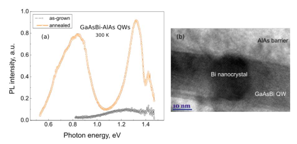
Firstly, PL spectra of as-grown and annealed at 750°C temperature GaAsBi/AlAs QWs structures were compared (see Fig. 1(a)). PL spectra showed that thermal annealing of GaAsBi/AlAs QWs sample induced increase of PL intensity and appearance of additional PL peak at low energies. This peak was attributed to Bi nanoclusters. Furthermore, HRTEM (Fig. 1(b)) and Raman scattering measurements evidenced that these nanoclusters are predominantly composed of Bi atoms. Low-temperature PL spectra of GaAsBi/AlAs structure containing 10 nm- and 20 nm-width QWs showed that PL band related to Bi nanocrystals is rather complex; it is composed of several separate peaks with distinguished photon energies at 0.67 eV, 0.88 eV and 0.98 eV (spectrum at 3 K temperature). These peaks were assigned to Bi nanoparticles with various sizes, which formed in 10 nm- and 20 nm-width QWs. That indicates that GaAsBi/AlAs QW width possibly sets size of Bi nanoclusters, which forms after thermal annealing.