InGaN has a direct band gap that covers the range from 0.65 to 3.4 eV, depending on indium content. Technically, InGaN is suitable for light emitting diodes (LED) emitting in the entire visible spectrum [1]; however, it is increasingly difficult to achieve an efficient yellow or red InGaN-based LED, a problem known as a green gap [2]. The green gap is caused mainly by decreasing material structural quality and increasing internal electric field, as indium content is increased [3]. Therefore, an improvement of growth techniques, allowing for higher quality InGaN layers, is in great demand. In this work, we study the impact of interrupted metalorganic chemical vapor deposition (MOCVD) growth method on InGaN electrical properties.
6 InGaN quantum well structures were grown by interrupted MOCVD method on c-plane sapphire substrates. The samples were grown by varying the duration of interruptions of metal precursor flow during the InGaN well growth; all samples are consisted of five InGaN quantum wells (QWs), separated by a several times thicker GaN quantum barrier (QB) [4]. For measurements, we used the differential transmission (DT) and photoluminescence (PL) techniques. For the evaluation of PL quantum efficiency (QE) we applied the three-measurement approach with an integrating sphere [5].
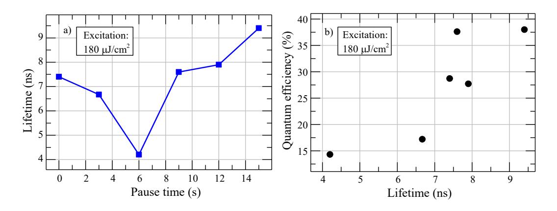
We demonstrate that the carrier lifetime increases with the increasing duration of metal precursor flow interruption (Fig. 1a). This can be a result of a more homogeneous distribution of indium atoms on the growth surface during the longer pause. We also show that longer lifetime results in higher quantum efficiency of the quantum well structure (Fig. 1b). This correlation points out to lower defect density in the samples grown with longer interruptions of metal precursor flow. On the negative side, a longer interruptions result in blue shift of PL spectra, probably due partial evaporation of indium atoms.