
Transition-metal dichalcogenide crystals (TMDCs) have emerged as a new class of materials that display exceptional physical and optical properties [1]. Thickness is one of the fundamental parameters that define their surprising and unique electronic properties. Monolayer of this materials have the direct bandgap which gives an advantage over the indirect bandgap in bulk TMDCs, thus makes them promising candidates for several interesting applications as light emitters, detectors, and photovoltaic devices [2].
One of the typical representative compound of the TMDCs family is molybdenum diselenide (MoSe2), a synthetic crystal, which structure is characterized by strong intralayer covalent bonds within planes of hexagonally arranged between selenium and molybdenum atoms and by weak out-of-plane van der Waals interactions Se-Mo-Se layers [3].
It's important for applications and research purposes to have easy, quick and nondestructive method of determination of layer thickness. Optical microscopy can give inconclusive results, we propose using two different wavelengths in order to effectively determine number of layers of TMDCs and visualize defects. A confocal microscope was used for scanning the surface of MoSe2 samples and for studying different defects formed during the exfoliation process. The measurements were carried out at room temperature using red (650 nm) and green (532 nm) laser light illumination. With increasing thickness of the sample the change of the relative reflection was observed. We use characteristic difference of relative reflections to determine the exact number of TMDC layers. This method provides also a quick method of visualization of the presence of defects of 2D materials.
We verified the experimental results by Raman spectroscopy. The energy difference between $E_{2g}^{1}$ (active out-of plane vibrational mode), $A_{1g}$ (active in-plane vibrational mode) and $B_{2g}^{1}$ (inactive in-plane vibrational mode) allowed for independent measurement of the thickness of our sample. A key role is played by the intensity and shape of the peaks in the Raman scattering.
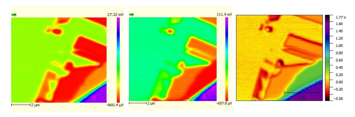
The new method was checked by theoretical model. We used transfer matrix method to obtain dependence between the number of MoSe2 layers and the intensity of reflected light. Main parameters of the model was thicknesses of materials, their indices of refraction at the given wavelength of light. Consistency of experiment and theoretical model was confirmed.