
Sub-wavelength periodic structures, also known as metamaterials, are uniquely designed structures that allow us to manipulate the electromagnetic waves and their properties. This brings us the capabilities of engineering specific devices including but not limited to sensors, filters and others for many promising applications [1].
The very first demonstration of the possibilities emerged in 1998, while using sub-wavelength apertures in a metal previously unpredicted spectral lines were observed [2]. Following experiments proved that such spectra can be adjusted by exploring different parameters of material, but more importantly the distribution and the geometrical size of the structures, making the structures not just wavelength but polarization dependent as well. Main explanation of the phenomena comes from the surface working as a grating and the resonances due to the coupling of electromagnetic wave to the oscillations of the free electrons at the surface of metal, so called plasmons. It should be noted that in the recent year it was proved that dielectric materials might also be used for the above mentioned manipulation of light.
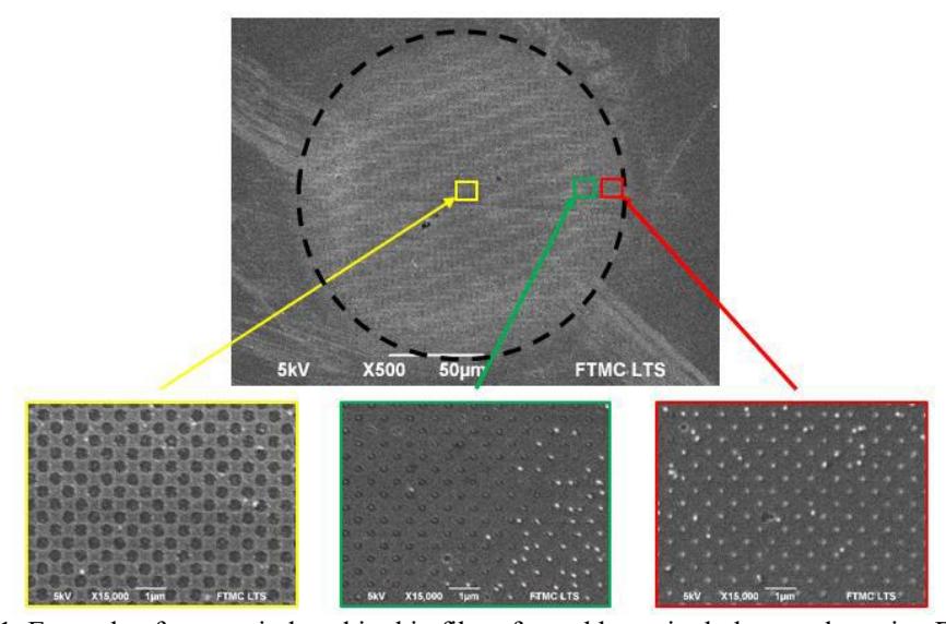
Apart from the work done towards understanding of light propagation, the fabrication by using Direct Laser Interference Patterning (DLIP) was carried out. Even-though there has been some work done with DLIP before, the period of formed structures were in the range of μm [3], thus, for the first time to our knowledge, we suggest such method for structuring of plasmonic materials. DLIP was used to pattern thin-films of different types of metal: chromium (Cr), gold (Au) and niobium (Nb). Samples of different thickness (5-100 nm) were analysed and the ablation compared to theoretical predictions. The experiments proved that DLIP method is capable of structuring 600 nm period apertures in Cr and Nb while the method is limited in Au due to thermal processes and this should be further investigated. The study of topology (Fig. 1) as well as the structural dependence on laser parameters: pulse energy and number of pulses, were carried out in order to optimise the effectiveness of laser processing.
Light propagation through the structures can be determined by various computational techniques, including the Finite Element Method (FEM) in COMSOL Multiphysics program package, solving partial differential equations. Modelling is critically connected to a proper setting of boundary conditions, properties of materials and description of propagating electromagnetic wave. Results comparable to experimental data can be successfully obtained while changing wide range of parameters: chosen material, periodic arrangement, size and form, as well as the angle of incidence and surrounding environment.
In the scope of this work, dielectric sub-wavelength structures will also be discussed. Appearance of such loss-less structures provides a lot of benefits compared to the metallic ones while sustaining the abilities of manipulation of light, though the usage of DLIP is not a solution for the fabrication of such structures. The metasurfaces based on silicon (Si) nanostructures are extremely promising in the field of multi-dimensional imaging.