Combining a nanomanipulation and electrical measurement set-up together with real-time visualization provides a powerful tool for control and investigation of processes occurring at the nanoscale.
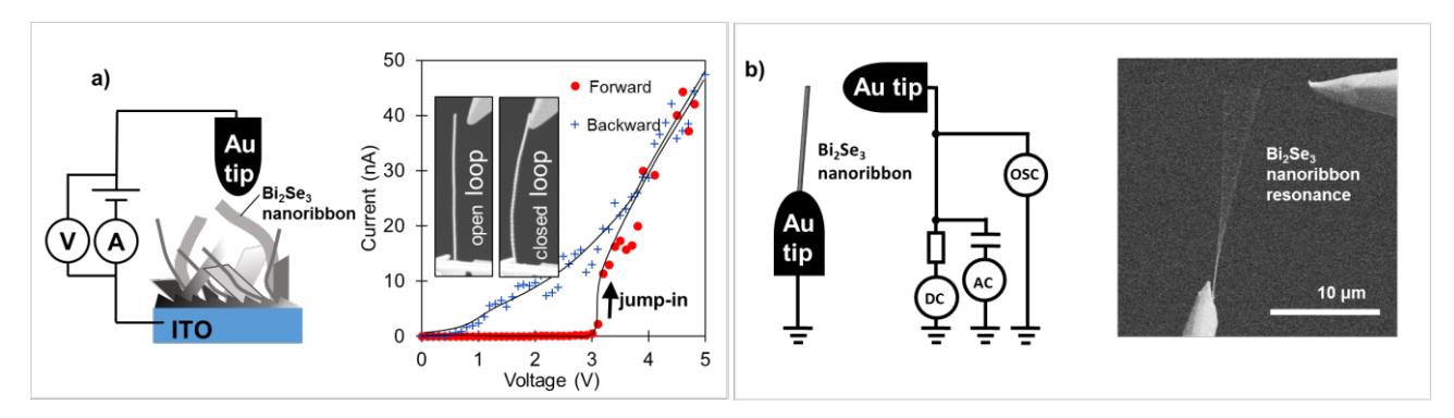
We will present an experimental approach for characterization of nanostructures and their electrical and mechanical properties by in-situ scanning electron microscopy (SEM). One-dimensional bismuth selenide (Bi2Se3) nanostructures – nanoribbons, have thermoelectric and topological insulator properties, prospective for applications in energy conversion, as well as spintronic and quantum information devices. Besides, due to their size, shape, and elasticity, they can act as active elements in nanoelectromechanical systems and sensors. We investigate nanoelectromechanical switching and electrical breakdown parameters of individual Bi2Se3 nanoribbons, analyze their vibrations and finally, determine the Young's modulus.
Experiments are performed in-situ SEM Hitachi S-4800. The set-up is configured using a Smaract 13D nanomanipulation system and Au tips, which are used as electrodes for electrical measurements (Fig. 1a) and electrostatic excitation of the nanoribbon resonance (Fig. 1b).
The results are important for interpretation of nanoscale processes, as well as characterization of nanomaterial properties and their application in nanodevices.