
Silicon carbide is very attractive material for microelectronic integrated circuits production due to chemical, electrical properties and also huge radiation and thermal durability. Silicon carbide substrates are expensive for serial production and it schould be found a method to growth defects free epitaxial silicon carbide layers on top of cheep silicon substrates. Silicon carbide layers grown directly on silicon are defect-riched due to significant lattice misfit and difference of thermal expansion coefficient [1]. Additionally, formation of porous layer under the silicon carbide results in decrease of elastic strain and consequently improves the structural quality of silicon carbide. One can suggest that additional growth of silicon-germanium (SiGe) buffer layer during SiC growth will leads to noticeable decrease of growth temperature as well as improvement of the quality of silicon carbide. The main goal of the present work is investigation of high temperature carbidization process of silicon wafers with epitaxial Si1-xGex buffer layers.
(111) Si wafers were used as substrates. The Si0.75Ge0.25 (15 nm)/SiC layers were grown by molecular beam epitaxy (MBE) onto Si wafers. The structural properties were investigated by bright-field and dark-field transmission electron microscopy (TEM) and electron diffraction analysis. The Raman spectroscopy (NanofinderHighEnd) spectrometer, excitation at 532 nm) was used for comparison.
Fig. 1 shows the TEM image of Si/ Si0.75Ge0.25 /SiC sample grown by MBE at 950 °C. Well visible bright areas in Fig. 1 are pores in SiGe layer because of SiC epi-growth. The pores formation apparently takes place due to Kirkendall effect. The faceted boundaries of several grains (Fig. 1) reveal the microtwins formation due to specific reflection of crystalline matrix or due to matrix rotation around its crystallographic axis. Raman spectrum shows typical optical and acustical vibration pikes for cubic phase of silicon carbide layers[2].
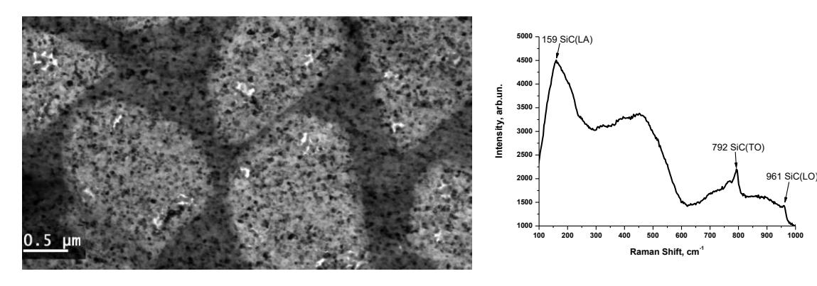
Using electron microscopy, electron diffraction and raman spectroscopy it was shown, that thermal treatment of Si\SiGe buffer structure at 950 °C in carbon atmosphere is followed by epitaxial growth of thin layers of cubic silicon carbide with high density of microtwins.