Layered van der Waals crystals are attracting increasing attention due to their unique chemical and physical properties. The discovery of quantum emission in hexagonal boron nitride (h-BN) in 2016 opens up applications in quantum computing, quantum communication, and nanoscale sensing [1]. The exact mechanism of the measured quantum emission from defects in h-BN remains unclear.
Native point defects and impurities have been extensively studied using quantum chemistry calculations to determine the potential candidates of observed quantum emission [2]. Some experiments indicate that the observed luminescence may actually come from point defects located near line defects like grain boundaries and dislocations. These line defects are common in CVD-grown h-BN crystals. Using quantum chemistry calculations is too computationally expensive to model such large-scale systems. Therefore, the goal of the present work is to use force field (FF) methods to model these systems. In this study we have used the newest extended Tersoff potential for covalently bonded boron nitride systems and interlayer potential to model large-scale point defects and line defects in monolayer and bulk h-BN [3][4].
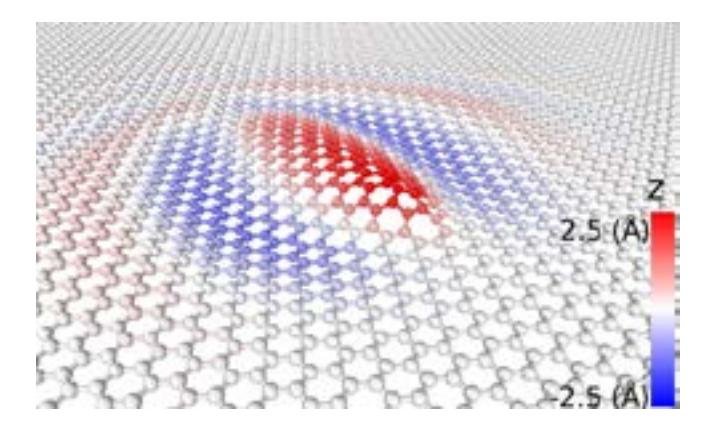
Various types of point and line defects have been created in monolayer and bulk h-BN crystals and we have performed energy minimization calculations to obtain optimized geometries. We have shown that crystal perturbations induced by line defects in 2D materials extend to very long distances. These crystal perturbations lead to variations of local defect geometries and thus also possibly to their optical signatures. These results will be later used in ab-initio calculations in our future works.